
1
Æ
FN6048.3
ISL8483E, ISL8485E
ESD Protected to ±15kV, 5V, Low Power,
High Speed or Slew Rate Limited,
RS-485/RS-422 Transceivers
These Intersil RS-485/RS-422 devices are ESD protected,
BiCMOS 5V powered, single transceivers that meet both the
RS-485 and RS-422 standards for balanced communication.
Each driver output/receiver input is protected against ±15kV
ESD strikes, without latch-up. Unlike competitive devices,
this Intersil family is specified for 10% tolerance supplies
(4.5V to 5.5V).
The ISL8483E utilizes slew rate limited drivers which reduce
EMI, and minimize reflections from improperly terminated
transmission lines, or unterminated stubs in multidrop and
multipoint applications.
Data rates up to 5Mbps are achievable by using the
ISL8485E which features higher slew rates.
Both devices present a "single unit load" to the RS-485 bus,
which allows up to 32 transceivers on the network.
Receiver (Rx) inputs feature a "fail-safe if open" design,
which ensures a logic high Rx output, if Rx inputs are
floating.
Driver (Tx) outputs are short circuit protected, even for
voltages exceeding the power supply voltage. Additionally,
on-chip thermal shutdown circuitry disables the Tx outputs to
prevent damage if power dissipation becomes excessive.
These half duplex configurations multiplex the Rx inputs and
Tx outputs to allow transceivers with Rx and Tx disable
functions in 8 lead packages.
Features
∑ RS-485 I/O Pin ESD Protection
. . . . . . . . . . . . . ±
15kV HBM
- Class 3 ESD Level on all Other Pins . . . . . . >7kV HBM
∑ Specified for 10% Tolerance Supplies
∑ High Data Rate Version (ISL8485E) . . . . . . up to 5Mbps
∑ Slew Rate Limited Version for Error Free Data
Transmission (ISL8483E) . . . . . . . . . . . . . .up to 250kbps
∑ Single Unit Load Allows up to 32 Devices on the Bus
∑ 1nA Low Current Shutdown Mode (ISL8483E)
∑ Low Quiescent Current:
- 160
µ
A (ISL8483E)
- 340
µ
A (ISL8485E)
∑ -7V to +12V Common Mode Input Voltage Range
∑ Three State Rx and Tx Outputs
∑ 30ns Propagation Delays, 5ns Skew (ISL8485E)
∑ Operate from a Single +5V Supply (10% Tolerance)
∑ Current Limiting and Thermal Shutdown for driver
Overload Protection
Applications
∑ Factory Automation
∑ Security Networks
∑ Building Environmental Control Systems
∑ Industrial/Process Control Networks
∑ Level Translators (e.g., RS-232 to RS-422)
∑ RS-232 "Extension Cords"
TABLE 1. SUMMARY OF FEATURES
PART
NUMBER
HALF/FULL
DUPLEX
NO. OF DEVICES
ALLOWED ON BUS
DATA RATE
(Mbps)
SLEW-RATE
LIMITED?
RECEIVER/DRIVER
ENABLE?
QUIESCENT
I
CC
(
µ
A)
LOW POWER
SHUTDOWN?
PIN
COUNT
ISL8483E
Half
32
0.25
Yes
Yes
160
Yes
8
ISL8485E
Half
32
5
No
Yes
340
No
8
Data Sheet
December 2003
CAUTION: These devices are sensitive to electrostatic discharge; follow proper IC Handling Procedures.
1-888-INTERSIL or 321-724-7143
|
Intersil (and design) is a registered trademark of Intersil Americas Inc.
Copyright © Intersil Americas Inc. 2003. All R ights Reserved.
All other trademarks mentioned are the property of their respective owners.

2
Pinout
ISL8483E, ISL8485E (PDIP, SOIC)
TOP VIEW
RO
RE
DE
DI
1
2
3
4
8
7
6
5
V
CC
B / Z
A / Y
GND
D
R
Ordering Information
PART NO.
(BRAND)
TEMP.
RANGE (
o
C)
PACKAGE
PKG. DWG. #
ISL8483EIB
(8483EIB)
-40 to 85
8 Ld SOIC
M8.15
ISL8483EIB-T
(8483EIB)
-40 to 85
8 Ld SOIC
Tape and Reel
M8.15
ISL8483EIP
-40 to 85
8 Ld PDIP
E8.3
ISL8485ECB
(8485ECB)
0 to 70
8 Ld SOIC
M8.15
ISL8485ECB-T
(8485ECB)
0 to 70
8 Ld SOIC
Tape and Reel
M8.15
ISL8485ECP
0 to 70
8 Ld PDIP
E8.3
ISL8485EIB
(8485EIB)
-40 to 85
8 Ld SOIC
M8.15
ISL8485EIB-T
(8485EIB)
-40 to 85
8 Ld SOIC
Tape and Reel
M8.15
ISL8485EIP
-40 to 85
8 Ld PDIP
E8.3
Truth Tables
TRANSMITTING
INPUTS
OUTPUTS
RE
DE
DI
Z
Y
X
1
1
0
1
X
1
0
1
0
0
0
X
High-Z
High-Z
1
0
X
High-Z *
High-Z *
*Shutdown Mode for ISL8483E (see Note 7)
RECEIVING
INPUTS
OUTPUT
RE
DE
A-B
RO
0
0
+0.2V
1
0
0
-0.2V
0
0
0
Inputs Open
1
1
0
X
High-Z*
1
1
X
High-Z
*Shutdown Mode for ISL8483E (see Note 7)
Pin Descriptions
PIN
FUNCTION
RO
Receiver output: If A > B by at least 0.2V, RO is high; If A < B by 0.2V or more, RO is low; RO = High if A and B are unconnected (floating).
RE
Receiver output enable. RO is enabled when RE is low; RO is high impedance when RE is high.
DE
Driver output enable. The driver outputs, Y and Z, are enabled by bringing DE high. They are high impedance when DE is low.
DI
Driver input. A low on DI forces output Y low and output Z high. Similarly, a high on DI forces output Y high and output Z low.
GND
Ground connection.
A/Y
±15kV HBM ESD Protected, RS-485/422 level noninverting receiver input and noninverting driver output. Pin is an input (A) if DE = 0;
pin is an output (Y) if DE = 1.
B/Z
±15kV HBM ESD Protected, RS-485/422 level inverting receiver input and inverting driver output. Pin is an input (B) if DE = 0; pin is
an output (Z) if DE = 1.
V
CC
System power supply input (4.5V to 5.5V).
ISL8483E, ISL8485E

3
Typical Operating Circuits
ISL8483E, ISL8485E
0.1
µ
F
+
D
R
7
6
8
1
2
3
4
5
V
CC
GND
RO
RE
DE
DI
A / Y
B / Z
+5V
0.1
µ
F
+
D
R
6
7
8
1
2
3
4
5
V
CC
GND
RO
RE
DE
DI
A / Y
B / Z
+5V
R
T
R
T
ISL8483E, ISL8485E

4
Absolute Maximum Ratings
Thermal Information
V
CC
to Ground. . . . . . . . . . . . . . . . . . . . . . . . . . . . . . . . . . . . . . . 7V
Input Voltages
DI, DE, RE . . . . . . . . . . . . . . . . . . . . . . . . . . -0.5V to (V
CC
+0.5V)
Input / Output Voltages
A/Y, B/Z . . . . . . . . . . . . . . . . . . . . . . . . . . . . . . . . . -8V to +12.5V
RO . . . . . . . . . . . . . . . . . . . . . . . . . . . . . . . . -0.5V to (V
CC
+0.5V)
Short Circuit Duration
Y, Z. . . . . . . . . . . . . . . . . . . . . . . . . . . . . . . . . . . . . . . Continuous
ESD Rating . . . . . . . . . . . . . . . . . . . . . . . . . See Specification Table
Operating Conditions
Temperature Range
ISL8485ECX. . . . . . . . . . . . . . . . . . . . . . . . . . . . . . . 0
o
C to 70
o
C
ISL848XEIX . . . . . . . . . . . . . . . . . . . . . . . . . . . . . . -40
o
C to 85
o
C
Thermal Resistance (Typical, Note 1)
JA
(
o
C/W)
8 Ld SOIC Package . . . . . . . . . . . . . . . . . . . . . . . . .
170
8 Ld PDIP Package . . . . . . . . . . . . . . . . . . . . . . . . .
140
Moisture Sensitivity (see Technical Brief TB363)
All Packages . . . . . . . . . . . . . . . . . . . . . . . . . . . . . . . . . . . Level 1
Maximum Junction Temperature (Plastic Package) . . . . . . . 150
o
C
Maximum Storage Temperature Range . . . . . . . . . -65
o
C to 150
o
C
Maximum Lead Temperature (Soldering 10s) . . . . . . . . . . . . 300
o
C
(SOIC - Lead Tips Only)
CAUTION: Stresses above those listed in "Absolute Maximum Ratings" may cause permanent damage to the device. This is a stress only rating and operation of the
device at these or any other conditions above those indicated in the operational sections of this specification is not implied.
NOTE:
1.
JA
is measured with the component mounted on a low effective thermal conductivity test board in free air. See Tech Brief TB379 for details.
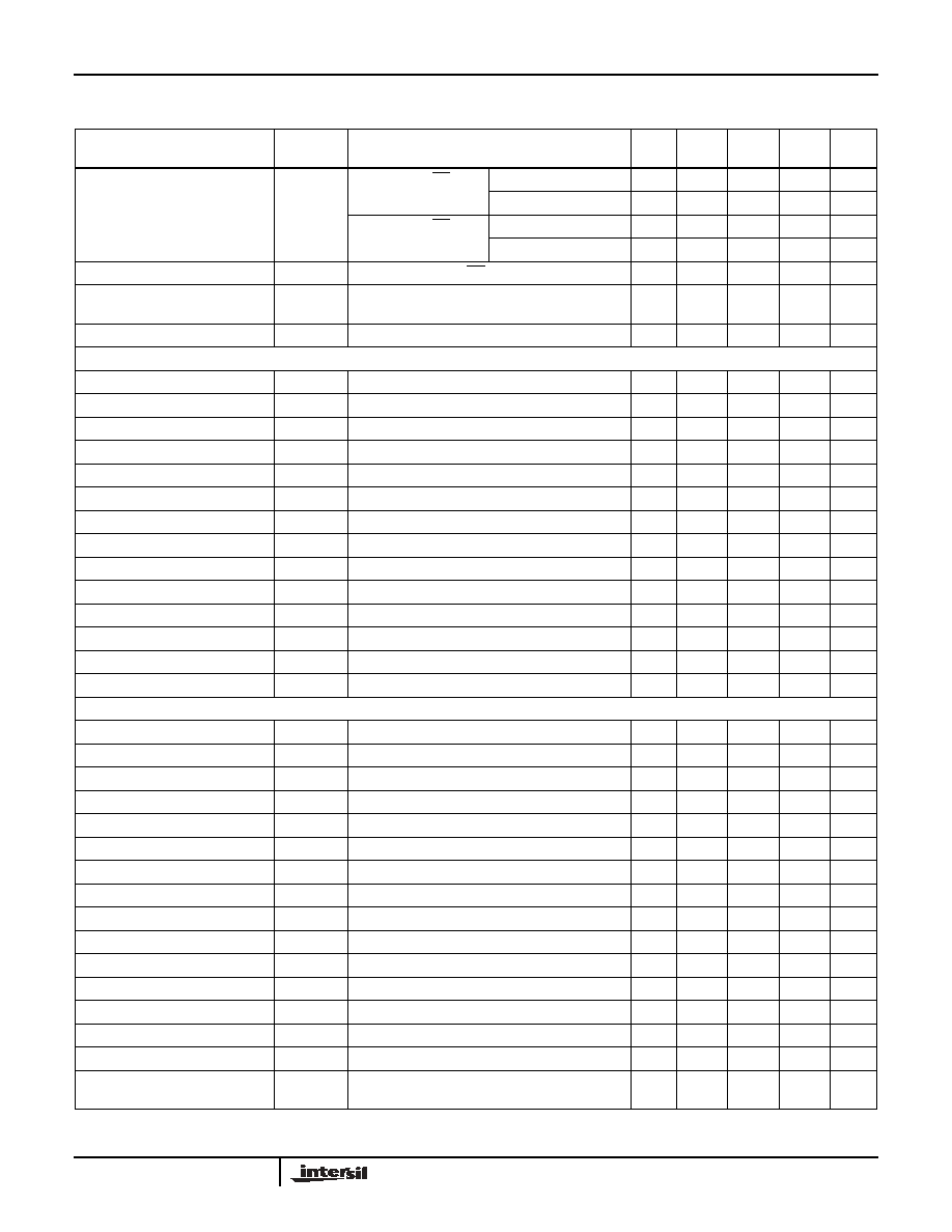
Electrical Specifications
Test Conditions: V
CC
= 4.5V to 5.5V; Unless Otherwise Specified.
Typicals are at V
CC
= 5V, T
A
= 25
o
C, (Note 2)
PARAMETER
SYMBOL
TEST CONDITIONS
TEMP
(
o
C)
MIN
TYP
MAX
UNITS
DC CHARACTERISTICS
Driver Differential V
OUT
(no load)
V
OD1
Full
-
-
V
CC
V
Driver Differential V
OUT
(with load)
V
OD2
R = 50
(RS-422), (Figure 1)
Full
2
3
-
V
R = 27
(RS-485), (Figure 1)
Full
1.5
2.3
5
V
Change in Magnitude of Driver
Differential V
OUT
for
Complementary Output States
V
OD
R = 27
or 50
, (Figure 1)
Full
-
0.01
0.2
V
Driver Common-Mode V
OUT
V
OC
R = 27
or 50
, (Figure 1)
Full
-
-
3
V
Change in Magnitude of Driver
Common-Mode V
OUT
for
Complementary Output States
V
OC
R = 27
or 50
, (Figure 1)
Full
-
0.01
0.2
V
Logic Input High Voltage
V
IH
DE, DI, RE
Full
2
-
-
V
Logic Input Low Voltage
V
IL
DE, DI, RE
Full
-
-
0.8
V
Logic Input Current
I
IN1
DE, DI, RE (ISL8483E)
Full
-2
-
2
µ
A
I
IN1
DI (ISL8485E
)
Full
-2
-
2
µ
A
I
IN1
DE,
RE (ISL8485E)
Full
-25
-
25
µ
A
Input Current (A, B), (Note 10)
I
IN2
DE = 0V, V
CC
= 0V or
4.5 to 5.5V
V
IN
= 12V
Full
-
-
1
mA
V
IN
= -7V
Full
-
-
-0.8
mA
Receiver Differential Threshold
Voltage
V
TH
-7V
V
CM
12V
Full
-0.2
-
0.2
V
Receiver Input Hysteresis
V
TH
V
CM
= 0V
25
-
70
-
mV
Receiver Output High Voltage
V
OH
I
O
= -4mA, V
ID
= 200mV
Full
3.5
-
-
V
Receiver Output Low Voltage
V
OL
I
O
= -4mA, V
ID
= 200mV
Full
-
-
0.4
V
Three-State (high impedance)
Receiver Output Current
I
OZR
0.4V
V
O
2.4V
Full
-
-
±
1
µ
A
Receiver Input Resistance
R
IN
-7V
V
CM
12V
Full
12
-
-
k
ISL8483E, ISL8485E
5
No-Load Supply Current, (Note 3)
I
CC
ISL8485E, DI, RE = 0V
or V
CC
DE = V
CC
Full
-
550
900
µ
A
DE = 0V
Full
-
340
500
µ
A
ISL8483E, DI, RE = 0V
or V
CC
DE = V
CC
Full
-
390
650
µ
A
DE = 0V
Full
-
160
250
µ
A
Shutdown Supply Current
I
SHDN
ISL8483E, DE = 0V, RE = V
CC
, DI = 0V or V
CC
Full
-
1
50
nA
Driver Short-Circuit Current,
V
O
= High or Low
I
OSD1
DE = V
CC
, -7V
V
Y
or V
Z
12V, (Note 4)
Full
35
-
250
mA
Receiver Short-Circuit Current
I
OSR
0V
V
O
V
CC
Full
7
-
85
mA
SWITCHING CHARACTERISTICS (ISL8485E)
Driver Input to Output Delay
t
PLH
, t
PHL
R
DIFF
= 54
, C
L
= 100pF, (Figure 2)
Full
18
30
50
ns
Driver Output Skew
t
SKEW
R
DIFF
= 54
, C
L
= 100pF, (Figure 2)
Full
-
2
10
ns
Driver Differential Rise or Fall Time
t
R
, t
F
R
DIFF
= 54
, C
L
= 100pF, (Figure 2)
Full
3
11
25
ns
Driver Enable to Output High
t
ZH
C
L
= 100pF, SW = GND, (Figure 3)
Full
-
17
70
ns
Driver Enable to Output Low
t
ZL
C
L
= 100pF, SW = V
CC
, (Figure 3)
Full
-
14
70
ns
Driver Disable from Output High
t
HZ
C
L
= 15pF, SW = GND, (Figure 3)
Full
-
19
70
ns
Driver Disable from Output Low
t
LZ
C
L
= 15pF, SW = V
CC
, (Figure 3)
Full
-
13
70
ns
Receiver Input to Output Delay
t
PLH
, t
PHL
(Figure 4)
Full
30
40
150
ns
Receiver Skew | t
PLH
- t
PHL
|
t
SKD
(Figure 4)
25
-
5
-
ns
Receiver Enable to Output High
t
ZH
C
L
= 15pF, SW = GND, (Figure 5)
Full
-
9
50
ns
Receiver Enable to Output Low
t
ZL
C
L
= 15pF, SW = V
CC
, (Figure 5)
Full
-
9
50
ns
Receiver Disable from Output High
t
HZ
C
L
= 15pF, SW = GND, (Figure 5)
Full
-
9
50
ns
Receiver Disable from Output Low
t
LZ
C
L
= 15pF, SW = V
CC
, (Figure 5)
Full
-
9
50
ns
Maximum Data Rate
f
MAX
Full
5
-
-
Mbps
SWITCHING CHARACTERISTICS (ISL8483E)
Driver Input to Output Delay
t
PLH
, t
PHL
R
DIFF
= 54
, C
L
= 100pF, (Figure 2)
Full
250
800
2000
ns
Driver Output Skew
t
SKEW
R
DIFF
= 54
, C
L
= 100pF, (Figure 2)
Full
-
160
800
ns
Driver Differential Rise or Fall Time
t
R
, t
F
R
DIFF
= 54
, C
L
= 100pF, (Figure 2)
Full
250
800
2000
ns
Driver Enable to Output High
t
ZH
C
L
= 100pF, SW = GND, (Figure 3), (Note 5)
Full
250
-
2000
ns
Driver Enable to Output Low
t
ZL
C
L
= 100pF, SW = V
CC
, (Figure 3), (Note 5)
Full
250
-
2000
ns
Driver Disable from Output High
t
HZ
C
L
= 15pF, SW = GND, (Figure 3)
Full
300
-
3000
ns
Driver Disable from Output Low
t
LZ
C
L
= 15pF, SW = V
CC
, (Figure 3)
Full
300
-
3000
ns
Receiver Input to Output Delay
t
PLH
, t
PHL
(Figure 4)
Full
250
350
2000
ns
Receiver Skew | t
PLH
- t
PHL
|
t
SKD
(Figure 4)
25
-
25
-
ns
Receiver Enable to Output High
t
ZH
C
L
= 15pF, SW = GND, (Figure 5), (Note 6)
Full
-
10
50
ns
Receiver Enable to Output Low
t
ZL
C
L
= 15pF, SW = V
CC
, (Figure 5), (Note 6)
Full
-
10
50
ns
Receiver Disable from Output High
t
HZ
C
L
= 15pF, SW = GND, (Figure 5)
Full
-
10
50
ns
Receiver Disable from Output Low
t
LZ
C
L
= 15pF, SW = V
CC
, (Figure 5)
Full
-
10
50
ns
Maximum Data Rate
f
MAX
Full
250
-
-
kbps
Time to Shutdown
t
SHDN
(Note 7)
Full
50
200
600
ns
Driver Enable from Shutdown to
Output High
t
ZH(SHDN)
C
L
= 100pF, SW = GND, (Figure 3), (Notes 7, 8)
Full
-
-
2000
ns
Electrical Specifications
Test Conditions: V
CC
= 4.5V to 5.5V; Unless Otherwise Specified.
Typicals are at V
CC
= 5V, T
A
= 25
o
C, (Note 2) (Continued)
PARAMETER
SYMBOL
TEST CONDITIONS
TEMP
(
o
C)
MIN
TYP
MAX
UNITS
ISL8483E, ISL8485E