
1
Æ
FN8092.0
CAUTION: These devices are sensitive to electrostatic discharge; follow proper IC Handling Procedures.
1-888-INTERSIL or 1-888-468-3774
|
Intersil (and design) is a registered trademark of Intersil Americas Inc.
Copyright Intersil Americas Inc. 2005. All Rights Reserved
All other trademarks mentioned are the property of their respective owners.
ISL88705, ISL88706, ISL88707,
ISL88708, ISL88716, ISL88813
µP Supervisor with Watchdog Timer,
Power-Fail Comparator, Manual Reset and
Adjustable Power-On Reset
Designed with high reset threshold accuracy and low power
consumption, the ISL88705, ISL88706, ISL88707,
ISL88708, ISL88716 and ISL88813 devices are
microprocessor supervisors that are designed to monitor
power-supply and battery functions in microprocessor
systems. They can help to lower system cost, reduce board
space requirements and increase the reliability of systems.
These devices provide essential functions such as supply
voltage supervision by asserting a reset output during
power-up and power-down as well as during brownout
conditions. An auxiliary voltage monitor is provided for
detecting power failures warning the system of low battery
conditions or presence detection. In addition, an
independent watchdog timer helps to monitor
microprocessor activity every 1.6s (typical). An active-low
manual reset is offered and reset signals remain asserted
until V
DD
returns to proper operating levels.
Users can increase the nominal 200ms power-on reset time-
out delay by adding an external capacitor to the C
POR
pin on
the ISL88707 and ISL88708.
Features
∑ Fixed-Voltage Options Allow Precise Monitoring of +3.0V,
+3.3V, and +5.0V Power Supplies
∑ Additional Voltage Monitor for Power-Fail Detection or
Low-Battery Warning
- Monitors Voltages Down to 1.25V
- Adjustable Power-Fail Input Threshold
∑ Watchdog Timer Capability With 1.6s Time-out
∑ Both RST and RST Outputs Available
∑ 140ms Minimum Reset Pulse Width with Option to
Customize Using an External Capacitor
∑ Manual Reset Input On All Devices
∑ Reset Signal Valid Down to V
DD
= 1V
∑ Accurate ±1.8% Voltage Threshold
∑ Immune to Power-Supply Transients
∑ Ultra Low 10µA Maximum Supply Current at 3V
∑ Pb-Free Plus Anneal Available (RoHS Compliant)
Applications
∑ Portable/Battery Powered Equipment
∑ Notebook/Desktop Computer Systems
∑ Designs Using DSPs, Microcontrollers or Microprocessors
∑ Controllers
∑ Intelligent Instruments
∑ Communications Systems
∑ Industrial Equipment
Pinouts
ISL88705, ISL88706
(8 LD PDIP/SOIC)
TOP VIEW
ISL88716, ISL88813
(8 LD PDIP/SOIC)
TOP VIEW
ISL88707, ISL88708
(8 LD PDIP/SOIC)
TOP VIEW
1
2
3
4
8
7
6
5
V
DD
GND
PFI
WDO
RST
WDI
PFO
MR
1
2
3
4
8
7
6
5
V
DD
GND
PFI
WDO
RST
WDI
PFO
MR
1
2
3
4
8
7
6
5
V
DD
GND
PFI
RST
RST
C
POR
PFO
MR
Data Sheet
October 18, 2005

2
FN8092.0
October 18, 2005
Functional Block Diagrams
Ordering Information
PART NUMBER
(Notes 1, 2)
PART
MARKING
V
TH
TEMP
RANGE
(∞C)
PACKAGE
(Pb-Free)
ISL88705IP846Z ISL88705 Z I46 4.64V -40 to 85 8 Ld PDIP*
ISL88706IP844Z ISL88706 Z I44 4.38V -40 to 85 8 Ld PDIP*
ISL88706IP831Z ISL88706 Z I31 3.09V -40 to 85 8 Ld PDIP*
ISL88706IP829Z ISL88706 Z I29 2.92V -40 to 85 8 Ld PDIP*
ISL88706IP826Z ISL88706 Z I26 2.63V -40 to 85 8 Ld PDIP*
ISL88813IP846Z ISL88813 Z I46 4.64V -40 to 85 8 Ld PDIP*
ISL88716IP826Z ISL88716 Z I26 2.63V -40 to 85 8 Ld PDIP*
ISL88707IP846Z ISL88707 Z I46 4.64V -40 to 85 8 Ld PDIP*
ISL88708IP844Z ISL88708 Z I44 4.38V -40 to 85 8 Ld PDIP*
ISL88708IP831Z ISL88708 Z I31 3.09V -40 to 85 8 Ld PDIP*
ISL88708IP829Z ISL88708 Z I29 2.92V -40 to 85 8 Ld PDIP*
ISL88708IP826Z ISL88708 Z I26 2.63V -40 to 85 8 Ld PDIP*
ISL88705IB846Z
88705 Z I46
4.64V -40 to 85 8 Ld SOIC
ISL88706IB844Z
88706 Z I44
4.38V -40 to 85 8 Ld SOIC
ISL88706IB831Z
88706 Z I31
3.09V -40 to 85 8 Ld SOIC
ISL88706IB829Z
88706 Z I29
2.92V -40 to 85 8 Ld SOIC
ISL88706IB826Z
88706 Z I26
2.63V -40 to 85 8 Ld SOIC
ISL88813IB846Z
88813 Z I46
4.64V -40 to 85 8 Ld SOIC
ISL88716IB826Z
88716 Z I26
2.63V -40 to 85 8 Ld SOIC
ISL88707IB846Z
88707 ZI46
4.64V -40 to 85 8 Ld SOIC
ISL88708IB844Z
88708 Z I44
4.38V -40 to 85 8 Ld SOIC
ISL88708IB831Z
88708 Z I31
3.09V -40 to 85 8 Ld SOIC
ISL88708IB829Z
88708 Z I29
2.92V -40 to 85 8 Ld SOIC
ISL88708IB826Z
88708 Z I26
2.63V -40 to 85 8 Ld SOIC
NOTES:
1.
Add "-TK" suffix for SOIC Tape and Reel Packaging
2. Intersil Pb-free plus anneal products employ special Pb-free
material sets; molding compounds/die attach materials and
100% matte tin plate termination finish, which are RoHS
compliant and compatible with both SnPb and Pb-free soldering
operations. Intersil Pb-free products are MSL classified at
Pb-free peak reflow temperatures that meet or exceed the
Pb-free requirements of IPC/JEDEC J STD-020.
*Pb-free PDIPs can be used for through hole wave solder processing
only. They are not intended for use in Reflow solder processing
applications.
Ordering Information
(Continued)
PART NUMBER
(Notes 1, 2)
PART
MARKING
V
TH
TEMP
RANGE
(∞C)
PACKAGE
(Pb-Free)
± V
REF
V
DD
POR
GND
WDT
V
REF
PFI
WDI
PB
WDO
PF
PFO
MR
RST
ISL88705, ISL88706
V
REF
V
DD
POR
GND
WDT
V
REF
PFI
WDI
PB
WDO
PF
PFO
MR
RST
ISL88716, ISL88813
V
REF
V
DD
POR
GND
V
REF
PFI
PB
PF
PFO
MR
ISL88707, ISL88708
RST
RST
C
POR
OSC
±
±
±
±
±
ISL88705, ISL88706, ISL88707, ISL88708, ISL88716, ISL88813
3
FN8092.0
October 18, 2005
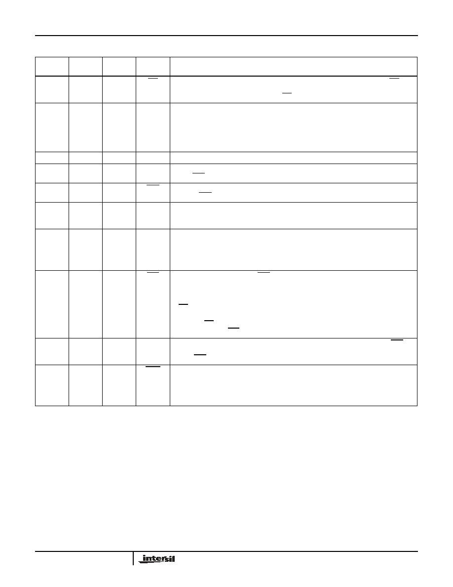
Pin Descriptions
ISL88705,
ISL88706
ISL88716,
ISL88813
ISL88707,
ISL88708
NAME
DESCRIPTION
1
1
1
MR
Manual Reset Input. A reset signal is generated when this input is pulled low.
The MR input
is an active low debounced input to which a user can connect a push-button to add manual
reset capability or drive with a signal. The MR pin has an internal 100k
pull-up.
2
2
2
V
DD
Power Supply Terminal. The voltage at this pin is compared against an internal factory-
programmed voltage trip point, V
TH1
. A reset is first asserted when the device is initially
powered up to ensure that the power supply has stabilized. Thereafter, reset is again asserted
whenever V
DD
falls below V
TH1
. The device is designed with hysteresis to help prevent
chattering due to noise and is immune to brief power-supply transients. The voltage threshold
V
TH1
is specified in the part number suffix.
3
3
3
GND
Ground Connection
4
4
4
PFI
Power-Fail Input This is an auxiliary monitored voltage input with a 1.25V threshold that
causes PFO state to follow the PFI input state.
5
5
5
PFO
Power-Fail Output. This output goes high if the voltage on PFI is greater than 1.25V,
otherwise PFO stays low.
6
C
POR
Adjustable POR Time-out Delay Input. Connecting an external capacitor from C
POR
to
ground allows the user to increase the Power On Reset timeout (t
POR
) from the nominal
200ms.
6
6
WDI
Watchdog Input. The Watchdog Input takes an input from a microprocessor and ensures that
it periodically toggles the WDI pin, otherwise the internal nominal 1.6s watchdog timer runs out,
then reset is asserted and WDO is pulled low. The internal Watchdog Timer is cleared
whenever the WDI sees a rising or falling edge or the device is manually reset. Floating WDI
or connecting WDI to a high-impedance three-state buffer disables the watchdog feature.
7
7
RST
Active-Low Reset Output. The RST output is an active low open drain output that is pulled
low to GND when reset is asserted. Reset is asserted whenever;
1. The device is first powered up,
2. V
DD
falls below its minimum voltage sense level or
3. MR is asserted.
The reset output continues to be asserted for typically 200ms after V
DD
rises above the reset
threshold or MR input goes from low to high. A watchdog time-out will not trigger a reset unless
WDO is connected to MR.
7
8
RST
Active-High Reset Output. The RST pin functions identically to its complementary RST
output but is an active high push pull output. RST is set high to V
DD
when reset is asserted.
See the RST description for more details on conditions that cause a reset.
8
8
WDO
Watchdog Output. This output is pulled low when the nominal 1.6s internal Watchdog Timer
expires and does not go high again until the watchdog is cleared. WDO also goes low during
low V
DD
conditions. Whenever V
DD
is below the reset threshold, WDO stays low. However,
unlike RESET, WDO does not have a minimum pulse width. As soon as V
DD
rises above the
reset threshold, WDO goes high with no delay.
ISL88705, ISL88706, ISL88707, ISL88708, ISL88716, ISL88813

4
FN8092.0
October 18, 2005
Absolute Maximum Ratings
Recommended Operating Conditions
Temperature Under Bias . . . . . . . . . . . . . . . . . . . . .-40∞C to +125∞C
Storage Temperature . . . . . . . . . . . . . . . . . . . . . . .-65∞C to +150∞C
Voltage on any Pin with Respect to GND . . . . . . . . . . . -1.0V to +7V
DC Output Current . . . . . . . . . . . . . . . . . . . . . . . . . . . . . . . . . . . 5mA
Lead Temperature (Soldering, 10s) . . . . . . . . . . . . . . . . . . . . . 300∞C
ESD Classification . . . . . . . . . . . . . . . . . . . . . . . . . . . . . .2.0kV HBM
200V MM
1kV CDM
Temperature Range (Industrial) . . . . . . . . . . . . . . . . . . -40∞C to 85∞C
CAUTION: Absolute Maximum Ratings indicate limits beyond which permanent damage to the device and impaired reliability may occur. These are stress ratings
provided for information only and functional operation of the device at these or any other conditions beyond those indicated in the operational sections of this
specification are not implied.
For guaranteed specifications and test conditions, see Electrical Specifications. The guaranteed specifications apply only for the test conditions listed. Some
performance characteristics may degrade when the device is not operated under the listed test conditions.
Electrical Specifications
Over the recommended operating conditions unless otherwise specified.
SYMBOL
PARAMETER
CONDITIONS
MIN
TYP
MAX
UNITS
V
DD
Supply Voltage Range
2.0
5.5
V
I
DD
V
DD
= 5V, WDT Inactive
10
19
µA
V
DD
= 3V, WDT Inactive
8
10
µA
I
LI
Input Leakage Current (PFI)
100
nA
I
LO
Output Leakage Current
100
nA
VOLTAGE THRESHOLDS
V
TH1
Fixed V
DD
Voltage Trip Point
4.556
4.640
4.724
V
4.301
4.380
4.459
V
3.034
3.090
3.146
V
2.867
2.920
2.973
V
2.583
2.630
2.677
V
V
TH1HYST
Hysteresis at V
TH1
Input
Temperature = 25∞C
V
TH1
= 4.64V
46
mV
V
TH1
= 4.38V
44
mV
V
TH1
= 3.09V
37
mV
V
TH1
= 2.92V
29
mV
V
TH1
= 2.63V
31
mV
RST AND RST
V
OL
Reset Output Voltage Low
V
DD
3.3V, Sinking 2.5mA
0.05
0.40
V
V
DD
< 3.3V, Sinking 1.5mA
0.05
0.40
V
V
OH
Reset Output Voltage High
V
DD
3.3V, Sourcing 2.5mA
V
DD
-0.6
V
DD
-0.4
V
V
DD
< 3.3V, Sourcing 1.5mA
V
DD
-0.6
V
DD
-0.4
V
t
RPD
V
TH
to Reset Asserted Delay
6
µs
t
POR
POR Time-Out Delay
C
POR
is open
140
200
260
ms
C
LOAD
Load Capacitance on Reset Pins
5
pF
MANUAL RESET
V
MRL
MR Input Voltage Low
0.8
V
V
MRH
MR Input Voltage High
V
DD
-0.6
V
t
MR
MR Minimum Pulse Width
550
ns
R
PU
Internal MR Pull-Up Resistor
20
k
ISL88705, ISL88706, ISL88707, ISL88708, ISL88716, ISL88813

5
FN8092.0
October 18, 2005
WATCHDOG TIMER (Note 3)
t
WDT
Watchdog Time-out Period
1.0
1.6
2.0
s
t
WDPS
WDI Minimum Pulse Width
100
ns
V
IL
Watchdog Input Voltage Low
0.3 x V
DD
V
V
IH
Watchdog Input Voltage High
0.7 x V
DD
V
V
WDOL
WDO Output Voltage Low
V
DD
3.3V, Sinking 2.5mA
0.05
0.40
V
V
DD
< 3.3V, Sinking 1.5mA
0.05
0.40
V
V
WDOH
WDO Output Voltage High
V
DD
3.3V, Sourcing 2.5mA
V
DD
-0.6
V
DD
-0.4
V
V
DD
< 3.3V, Sourcing 1.5mA
V
DD
-0.6
V
DD
-0.4
V
I
WDT
Watchdog Input Current
1
µA
POWER-FAIL DETECTION
V
THPFI
PFI Input Threshold Voltage
1.20
1.25
1.30
V
PFIV
THHYST
Hysteresis Voltage
20
mV
V
PFOL
PFO Output Voltage Low
V
DD
3.3V, Sinking 2.5mA
0.05
0.40
V
V
DD
< 3.3V, Sinking 1.5mA
0.05
0.40
V
V
PFOH
PFO Output Voltage High
V
DD
3.3V, Sourcing 2.5mA
V
DD
-0.6
V
DD
-0.4
V
V
DD
< 3.3V, Sourcing 1.5mA
V
DD
-0.6
V
DD
-0.4
V
NOTES:
3. Applies to ISL88705, ISL88706, ISL88716, and ISL88813.
Electrical Specifications
Over the recommended operating conditions unless otherwise specified. (Continued)
SYMBOL
PARAMETER
CONDITIONS
MIN
TYP
MAX
UNITS
Typical Performance Curves
FIGURE 1. PACKAGE POWER DISSIPATION vs AMBIENT
TEMPERATURE
FIGURE 2. PACKAGE POWER DISSIPATION vs AMBIENT
TEMPERATURE
JEDEC JESD51-3 LOW EFFECTIVE
THERMAL CONDUCTIVITY TEST BOARD
1.8
1.6
1.2
0.8
0.6
0.4
0.2
0
0
25
50
75
100
150
AMBIENT TEMPERATURE (∞C)
P
O
WER DIS
S
IPATION
(W)
85
1.25W
JA
= 100∞C/W
PDIP8
125
1.4
1
JEDEC JESD51-7 HIGH EFFECTIVE
THERMAL CONDUCTIVITY TEST BOARD
2
1.8
1.6
1.4
1.2
0.8
0.4
0
0
25
50
75
100
150
AMBIENT TEMPERATURE (∞C)
P
O
WER DIS
S
IPATION
(W)
85
1.471W
JA
= 85∞C/W
PDIP8
125
1
0.6
0.2
ISL88705, ISL88706, ISL88707, ISL88708, ISL88716, ISL88813