1
Æ
FN8137.0
CAUTION: These devices are sensitive to electrostatic discharge; follow proper IC Handling Procedures.
1-888-INTERSIL or 1-888-352-6832
|
Intersil (and design) is a registered trademark of Intersil Americas Inc.
Copyright Intersil Americas Inc. 2005. All Rights Reserved
All other trademarks mentioned are the property of their respective owners.
X60003B-50, X60003C-50, X60003D-50
Precision 5.0V SOT-23 FGATM Voltage
Reference
FEATURES
∑ Output Voltage: 5.000V
∑ Absolute Initial Accuracy Options:
±1.0mV, ±2.5mV, & ±5.0mV
∑ Ultra Low Power Supply Current: 500nA
∑ Low Temperature Coefficient Options:
10 & 20ppm/∞C
∑ 10 mA Source & Sink Current Capability
∑ 10 ppm/1000hrs Long Term Stability
∑ Very Low Dropout Voltage: 100 mV @ no load
∑ Supply Voltage Range: 5.1V to 9.0V
∑ 5kV ESD (Human Body Model)
∑ Standard Package: 3-lead SOT-23
∑ Temp Range: -40∞C to +85∞C
DESCRIPTION
The X60003x-50 FGATM voltage references are very
high precision analog voltage references fabricated in
Intersil's proprietary Floating Gate Analog technology,
which achieves superior levels of performance when
compared to conventional band gap, buried zener, or
X
FET
TM technologies.
FGATM voltage references feature very high initial
accuracy, very low temperature coefficient, excellent
long term stability, low noise and excellent line and
load regulation, at the lowest power consumption
currently available. These voltage references enable
advanced applications for precision industrial &
portable systems operating at significantly higher
accuracy and lower power levels than can be achieved
with conventional technologies.
APPLICATIONS
∑ High Resolution A/Ds & D/As
∑ Precision Current Sources
∑ Smart sensors
∑ Digital Meters
∑ Precision Regulators
∑ Strain Gage Bridges
∑ Calibration Systems
∑ Precision Oscillators
∑ Threshold Detectors
∑ V-F Converters
∑ Battery Management Systems
∑ Servo Systems
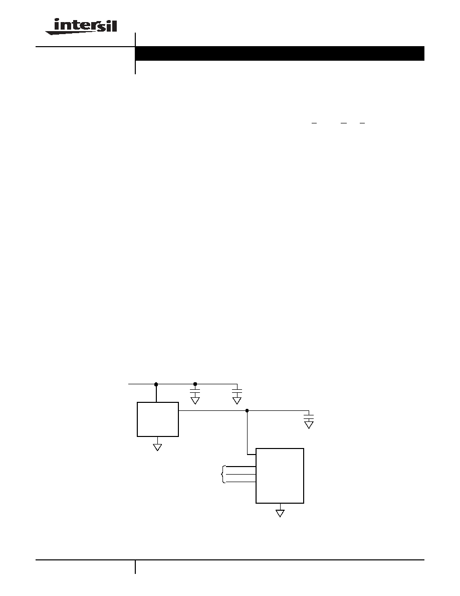
TYPICAL APPLICATION
V
IN
= +6.5V
0.1µF
Serial
Bus
V
IN
V
OUT
GND
X60003x-50
Enable
SCK
SDAT
A/D Converter
16 to 24-bit
REF IN
10µF
0.001µF
(
*
)
(
*
)
Also see Figure 3 in Applications Information
Data Sheet
March 15, 2005
2
FN8137.0
March 15, 2005
PACKAGE DIAGRAM
PIN CONFIGURATIONS
ORDERING INFORMATION
PART MARKING
Pin Name
Description
GND
Ground Connection
V
IN
Power Supply Input Connection
V
OUT
Voltage Reference Output Connection
1
2
3
SOT-23
V
OUT
X60003x-50
GND
V
IN
Order Part Number
Top Marking
X60003BIG3-50
AHA
X60003CIG3-50
AHB
X60003DIG3-50
AHC
Logo
Device Part Number
60003 = Standard
Grade
B = ±1.0 mV, 10 ppm/∞C
C = ±2.5 mV, 20 ppm/∞C
D = ±5.0 mV, 20 ppm/∞C
Temperature Range
I = -40∞C to +85∞C
Package
G3 = 3 lead SOT-23
V
OUT
Option
50 = 5.000V
X 60003 X I G3 ≠ 50
X60003B-50, X60003C-50, X60003D-50
3
FN8137.0
March 15, 2005
ABSOLUTE MAXIMUM RATINGS
Storage Temperature Range............ -65∞C to + 125∞C
Voltage on any Pin
Referenced to Gnd.............................-0.5V to + 10V
Lead Temperature (soldering, 10 secs).......... + 225∞C
RECOMMENDED OPERATING CONDITIONS
COMMENT
Absolute Maximum Ratings indicate limits beyond
which permanent damage to the device and impaired
reliability may occur. These are stress ratings provided
for information only and functional operation of the
device at these or any other conditions beyond those
indicated in the operational sections of this specifica-
tion are not implied.
For guaranteed specifications and test conditions, see
Electrical Characteristics.
The guaranteed specifications apply only for the test
conditions listed. Some performance characteristics
may degrade when the device is not operated under
the listed test conditions.
ELECTRICAL CHARACTERISTICS
(Operating Conditions: V
IN
= 6.5V, I
OUT
= 0mA, C
OUT
= 0.001µF, T
A
= -40 to +85∞C unless otherwise specified.)
Note:
1. Over the specified temperature range. Temperature coefficient is measured by the box method whereby the change in V
OUT
is divided
by the temperature range; in this case, -40∞C to +85∞C = 125∞C.
2. Thermal Hysteresis is the change in V
OUT
created by package stress @ T
A
= 25∞C after temperature cycling. V
OUT
is read initially at
T
A
= 25∞C; the X60003x-50 is then cycled between Hot (85∞C) and Cold (-40∞C) before a second V
OUT
measurement is taken at 25∞C.
The deviation between the initial V
OUT
reading and the second V
OUT
reading is then expressed in ppm.
3. Dropout voltage (V
DO
) is the minimum voltage (V
IN
) into the X60003x-50 which will produce the output voltage (
V
OUT
) drop specified
in the Electrical Characteristics table.
4. Guaranteed by Device Characterization
Temperature
Min.
Max.
Industrial
-40∞C
+85∞C
Symbol
Parameter
Conditions
Min
Typ
Max
Units
V
OUT
Output Voltage
5.000
V
V
OA
V
OUT
Accuracy
X60003B-50
X60003C-50
X60003D-50
T
A
= 25∞C
-1.0
-2.5
-5.0
+1.0
+2.5
+5.0
mV
I
IN
Supply Current
500
900
nA
V
IN
Input Voltage Range
5.1
9.0
V
TC V
OUT
Output Voltage
Temperature Coefficient
(1)
X60003B-50
X60003C-50
X60003D-50
10
20
20
ppm/
∞
C
V
OUT
/
V
IN
Line Regulation
+5.5V
V
IN
+8.0V
150
µ
V/V
V
OUT
/
I
OUT
Load Regulation
0mA
I
SOURCE
10mA
-10mA
I
SINK
0mA
10
20
50
100
µ
V/mA
V
OUT
/
t
Long Term Stability
T
A
= 25∞C
10
ppm/
1000Hrs
V
OUT
/
T
A
Thermal Hysteresis
(2)
T = -40
∞
C to +85
∞
C
100
ppm
V
DO
Dropout Voltage
(3)
I
OUT
= 5mA,
V
OUT
= -0.01%
150
300
mV
I
SC
Short Circuit Current
(4)
T
A
= 25∞C
50
80
mA
V
N
Output Voltage Noise
0.1Hz to 10Hz
30
µ
V
pp
X60003B-50, X60003C-50, X60003D-50

4
FN8137.0
March 15, 2005
TYPICAL PERFORMANCE CHARACTERISTIC CURVES
(V
IN
= 6.5V, I
OUT
= 0mA, T
A
= 25∞C unless otherwise specified)
+25
∞
C
+85
∞
C
-40
∞
C
Unit 3, I
IN
= 700nA
Unit 1, I
IN
= 350nA
Unit 2, I
IN
= 500nA
V
IN
(V)
V
IN
(V)
Delta V
OUT
(V)
(normailized to 5V at V
IN
= 6.5V)
Delta V
OUT
(
µ
V)
(normailized to V
IN
= 6.5V)
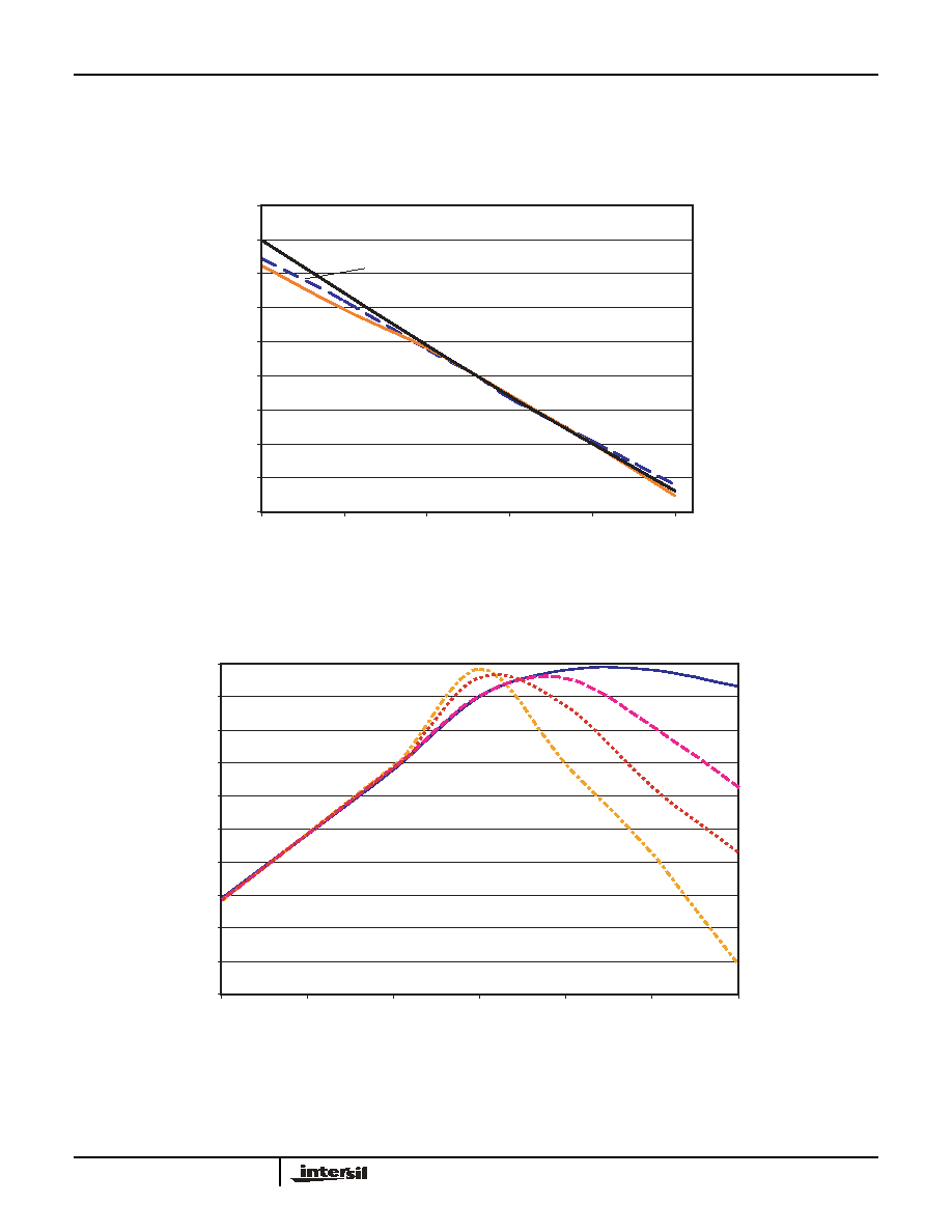
LINE REGULATION
-50
-25
0
25
50
75
100
125
150
5
6
7
8
9
LINE REGULATION
(3 Representative Units)
4.9997
4.9998
4.9999
5
5.0001
5.0002
5.0003
5
5.5
6
6.5
7
7.5
8
8.5
9
X60003B-50, X60003C-50, X60003D-50
5
FN8137.0
March 15, 2005
TYPICAL PERFORMANCE CHARACTERISTIC CURVES
(V
IN
= 6.5V, I
OUT
= 0mA, T
A
= 25∞C unless otherwise specified)
0.1Hz to 10Hz V
OUT
NOISE
1 Sec/div
10
µ
V/div
Band Pass Filter with 1 zero at .1Hz and 2 poles at 10 Hz
LOAD REGULATION
-0.40
0
-0.20
0.00
0.20
0.40
0.60
0.80
1.00
1.20
1.40
-20
-15
-10
-5
0
5
10
15
20
SINKING
OUTPUT CURRENT (mA)
SOURCING
DELTA Vout (mV)
-40
∞
C
+25
∞
C
+85
∞
C
+25
∞
C
X60003B-50, X60003C-50, X60003D-50
6
FN8137.0
March 15, 2005
TYPICAL PERFORMANCE CHARACTERISTIC CURVES
(V
IN
= 6.5V, I
OUT
= 0mA, T
A
= 25∞C unless otherwise specified)
FREQUENCY (Hz)
PSRR (dB)
V
OUT
vs TEMPERATURE
Normalized to 25
∞
C
(3 Representative Units)
4.998
4.9985
4.999
4.9995
5
5.0005
5.001
5.0015
5.002
5.0025
-40
-15
10
35
60
85
TEMPERATURE (
∞
C)
V
OUT
(V)
Unit 1, I
IN
= 350nA
Unit 2,
I
IN
= 500nA
Unit 3, I
IN
= 700nA
PSRR vs CAP Load
-100
-90
-80
-70
-60
-50
-40
-30
-20
-10
0
1
10
100
1000
10000
100000
1000000
No Load
1nF Load
10nF Load
100nF Load
X60003B-50, X60003C-50, X60003D-50
7
FN8137.0
March 15, 2005
TYPICAL PERFORMANCE CHARACTERISTIC CURVES
(V
IN
= 6.5V, I
OUT
= 0mA, T
A
= 25∞C unless otherwise specified)
10mA LOAD TRANSIENT RESPONSE
500mV/DIV
C
L
= .001
µ
F
I
IN
= -10mA
I
IN
= +10mA
2mSEC/DIV
50
µ
A LOAD TRANSIENT RESPONSE
100mV/DIV
500
µ
SEC/DIV
C
L
= .001
µ
F
I
IN
= -50
µ
A
I
IN
= +50
µ
A
LINE TRANSIENT RESPONSE
LINE TRANSIENT RESPONSE
200mV/DIV
500
µ
SEC/DIV
200mV/DIV
500
µ
SEC/DIV
C
L
= 0
C
L
= .001
µ
F
V
IN
= -500mV
V
IN
= +500mV
V
IN
= -500mV
V
IN
= +500mV
MINIMUM V
IN
to V
OUT
DIFFERENTIAL
OUTPUT CURRENT (Sourcing mA)
V
IN
to V
OUT
DIFFERENTIAL (V)
vs. OUTPUT CURRENT
-40
∞
C
+25
∞
C
+85
∞
C
0
0.05
0.1
0.15
0.2
0.25
0.3
0.35
0.4
0.45
0
2
4
6
8
10
X60003B-50, X60003C-50, X60003D-50
8
FN8137.0
March 15, 2005
TYPICAL PERFORMANCE CHARACTERISTIC CURVES
(V
IN
= 6.5V, I
OUT
= 0mA, T
A
= 25∞C unless otherwise specified)
Z
OUT
vs FREQUENCY
FREQUENCY (Hz)
Z
OUT
(
)
no Load
1nF Load
10nF Load
100nF Load
20
0
40
60
80
100
120
140
160
180
100
10
1
1000
10000
100000
5
5.5
6
6.5
7
7.5
8
8.5
9
9.5
I
IN
(nA)
V
IN
(V)
-40
∞
C
25
∞
C
85
∞
C
I
IN
vs V
IN
100
0
200
300
400
500
600
700
X60003B-50, X60003C-50, X60003D-50
9
FN8137.0
March 15, 2005
TYPICAL PERFORMANCE CHARACTERISTIC CURVES
(V
IN
= 6.5V, I
OUT
= 0mA, T
A
= 25∞C unless otherwise specified)
I
IN
(nA)
V
IN
(V)
Unit 1
Unit 2
Unit 3
I
IN
vs V
IN
(3 Representative Units)
0
100
200
300
400
500
600
700
800
900
5.0
6.0
7.0
8.0
9.0
10.0
TURN-ON TIME
0
0
2
4
6
8
10
12
1
2
3
4
5
6
TIME (mSec)
V
IN
& V
OUT
(V)
I
IN
= 500nA
X60003B-50, X60003C-50, X60003D-50

10
FN8137.0
March 15, 2005
APPLICATIONS INFORMATION
FGA Technology
The X60003x-50 voltage reference uses the floating
gate technology to create references with very low drift
and supply current. Essentially the charge stored on a
floating gate cell is set precisely in manufacturing. The
reference voltage output itself is a buffered version of
the floating gate voltage. The resulting reference device
has excellent characteristics which are unique in the
industry: very low temperature drift, high initial accu-
racy, and almost zero supply current. Also, the refer-
ence voltage itself is not limited by voltage bandgaps or
zener settings, so a wide range of reference voltages
can be programmed (standard voltage settings are pro-
vided, but customer-specific voltages are available).
The process used for these reference devices is a
floating gate CMOS process, and the amplifier circuitry
uses CMOS transistors for amplifier and output tran-
sistor circuitry. While providing excellent accuracy,
there are limitations in output noise level and load reg-
ulation due to the MOS device characteristics. These
limitations are addressed with circuit techniques dis-
cussed in other sections.
Nanopower Operation
Reference devices achieve their highest accuracy
when powered up continuously, and after initial stabili-
zation has taken place.
The X60003x-50 is the first high precision voltage ref-
erence with ultra low power consumption that makes it
practical to leave power-on continuously in battery
operated circuits. The X60003x-50 consumes
extremely low supply current due to the proprietary
FGA technology. Supply current at room temperature
is typically 500nA which is 1 to 2 orders of magnitude
lower than competitive devices. Application circuits
using battery power will benefit greatly from having an
accurate, stable reference which essentially presents
no load to the battery.
In particular, battery powered data converter circuits
that would normally require the entire circuit to be dis-
abled when not in use can remain powered up
between conversions as shown in figure 1. Data acqui-
sition circuits providing 12 to 24 bits of accuracy can
operate with the reference device continuously biased
with no power penalty, providing the highest accuracy
and lowest possible long term drift.
Other reference devices consuming higher supply cur-
rents will need to be disabled in between conversions
to conserve battery capacity. Absolute accuracy will
suffer as the device is biased and requires time to set-
tle to its final value, or, may not actually settle to a final
value as power-on time may be short.
Figure 1.
Board mounting Considerations
For applications requiring the highest accuracy, board
mounting location should be reviewed. Placing the
device in areas subject to slight twisting can cause
degradation of the accuracy of the reference voltage
due to die stresses. It is normally best to place the
device near the edge of a board, or the shortest side,
as the axis of bending is most limited at that location.
Obviously mounting the device on flexprint or
extremely thin PC material will likewise cause loss of
reference accuracy.
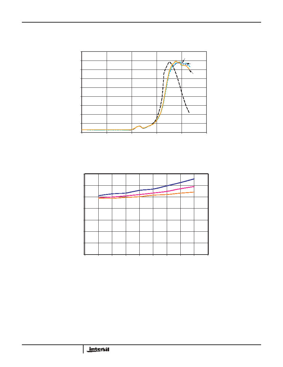
Noise Performance and Reduction:
The output noise voltage in a 0.1Hz to 10Hz
bandwidth is typically 30µVp-p. This is shown in the
plot in the Typical Performance Curves. The noise
measurement is made with a bandpass filter made of
a 1 pole high-pass filter with a corner frequency at
.1Hz and a 2-pole low-pass filter with a corner
frequency at 12.6Hz to create a filter with a 9.9Hz
bandwidth. Noise in the 10KHz to 1MHz bandwidth is
approximately 400µVp-p with no capacitance on the
output, as shown in Fig. 2 below. These noise
measurements are made with a 2 decade bandpass
filter made of a 1 pole high-pass filter with a corner
frequency at 1/10 of the center frequency and 1-pole
low-pass filter with a corner frequency at 10 times the
center frequency. Figure 2 also shows the noise in the
10KHz to 1MHz band can be reduced to about 50µVp-
p using a .001µF capacitor on the output. Noise in the
1KHz to 100KHz band can be further reduced using a
0.1µF capacitor on the output, but noise in the 1Hz to
100Hz band increases due to instability of the very low
power amplifier with a 0.1µF capacitance load. For
V
IN
= +6-9V
0.001µF
Serial
Bus
V
IN
V
OUT
GND
X60003x-50
REF IN
Enable
SCK
SDAT
A/D Converter
12 to 24-bit
0.01µF
10µF
X60003B-50, X60003C-50, X60003D-50

11
FN8137.0
March 15, 2005
load capacitances above .001µF the noise reduction
network shown in fig. 3 is recommended. This network
reduces noise sig-nificantly over the full bandwidth. As
shown in fig. 2, noise is reduced to less than 40µVp-p
from 1Hz to 1MHz using this network with a .01µF
capacitor and a 2k
resistor in series with a 10µF
capacitor.
Figure 2.
Figure 3.
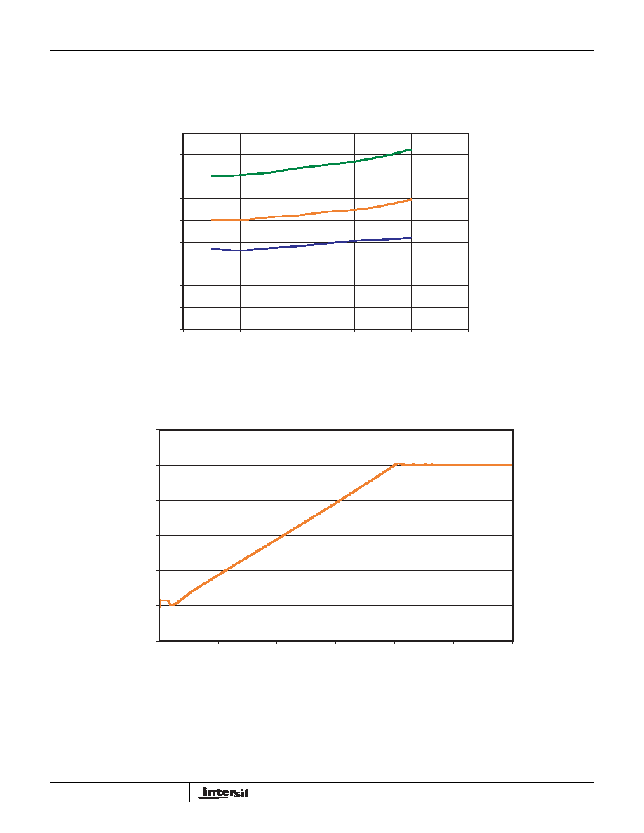
Turn-On Time
The X60003x-50 device has ultra-low supply current
and thus the time to bias up internal circuitry to final
values will be longer than with higher power refer-
ences. Normal turn-on time is typically 7ms. This is
shown in the graph, Figure 4. Since devices can vary
in supply current down to 300nA, turn-on time can last
up to about 12ms. Care should be taken in system
design to include this delay before measurements or
conversions are started.
Figure 4.
Temperature Coefficient
The limits stated for temperature coefficient (tempco)
are governed by the method of measurement. The
overwhelming standard for specifying the temperature
drift of a reference is to measure the reference voltage
at two temperatures, take the total variation, (V
HIGH
-
V
LOW
), and divide by the temperature extremes of
measurement (T
HIGH
- T
LOW
). The result is divided
by the nominal reference voltage (at T = 25∞C) and
multiplied by 10
6
to yield ppm/∞C. This is the "Box"
method for determining temperature coefficient.
CL = 0
CL = .001µF
CL = .1µF
CL = .01µF & 10µF + 2k
400
350
300
250
200
150
100
50
0
1
10
100
1000
10000
100000
X60003x-50 NOISE REDUCTION
NOISE VOLT
AGE (µ
Vp
-p
)
V
IN
= 6.5V
V
IN
V
O
GND
X60003x-50
.01µF
10µF
2k
.1µF
10µF
X60003 TURN-ON TIME (25
∞
C)
(3 Representative Units)
0
1
2
3
4
5
6
7
0
2
4
6
8
10
12
TIME (mSec)
V
IN
& V
OUT
(V)
I
IN
= 350nA
I
IN
= 500nA
I
IN
= 700nA
X60003B-50, X60003C-50, X60003D-50
12
FN8137.0
March 15, 2005
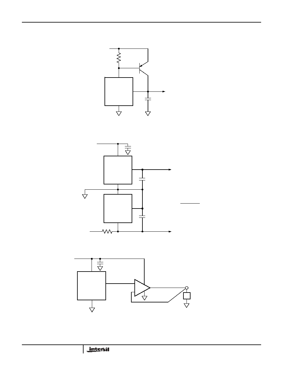
TYPICAL APPLICATION CIRCUITS
Precision 5V, 50mA Reference.
6V to 9V
2N2905
5.0V/50mA
0.001µF
V
IN
V
OUT
GND
X60003x-50
±5.0V Dual Output, High Accuracy Reference
V
IN
V
OUT
GND
GND
V
IN
V
OUT
X60003x-50
X60003x-50
0.1µF
0.001µF
5.0V
0.001µF
R
1
5.5V to 9V
V
IN
= -5.5V to -9.0V
-5.0V
; I
OUT
10mA
Kelvin Sensed Load
0.1µF
5.5V to 9V
V
IN
V
OUT
GND
X60003x-50
V
OUT
Sense
Load
R = 200
+
≠
5.0V - |
V
IN
|
R
1
=
-(I
OUT
)
X60003B-50, X60003C-50, X60003D-50

13
FN8137.0
March 15, 2005
TYPICAL APPLICATION CIRCUITS
-5.0V
R
1
Limits max load current
V
IN
V
OUT
GND
X60003x-50
C
IN
0.001
C
OUT
= 0.001µF
R
1
= 800
V
IN
= -9V
with R
I
= 800
, I
LOAD MAX
= 4mA
Negative Voltage Reference
V
IN
V
OUT
X60003x-50
GND
5.5V to 9V
0.1µF
0.001µF
V
OUT
+
≠
V
CC
R
H
R
L
X9119
V
SS
SDA
SCL
2-Wire Bus
V
OUT
(buffered)
5V Full Scale Low-Drift 10-bit Adjustable Voltage Source
5.0V - |
V
IN
|
R
1
=
-(I
OUT
)
X60003B-50, X60003C-50, X60003D-50

14
All Intersil U.S. products are manufactured, assembled and tested utilizing ISO9000 quality systems.
Intersil Corporation's quality certifications can be viewed at www.intersil.com/design/quality
Intersil products are sold by description only. Intersil Corporation reserves the right to make changes in circuit design, software and/or specifications at any time without
notice. Accordingly, the reader is cautioned to verify that data sheets are current before placing orders. Information furnished by Intersil is believed to be accurate and
reliable. However, no responsibility is assumed by Intersil or its subsidiaries for its use; nor for any infringements of patents or other rights of third parties which may result
from its use. No license is granted by implication or otherwise under any patent or patent rights of Intersil or its subsidiaries.
For information regarding Intersil Corporation and its products, see www.intersil.com
FN8137.0
March 15, 2005
PACKAGING INFORMATION
1. ALL DIMENSIONS IN INCHES (IN PARENTHESES IN MILLIMETERS)
2. PACKAGE DIMENSIONS EXCLUDE MOLDING FLASH
0.10 R MIN.
12∞ REF.
0.575 REF.
0.093 (2.35) BSC
3-Lead Plastic, SOT-23, Package Code G3
.024 (0.60)
.016 (0.40)
NOTES:
1
2
0.055 (1.40)
0.047 (1.20)
0.046 (1.18) BSC
0.075 (1.90) BSC
4X
0.35 H A-B D
2X N/2 TIPS
0.35 C A-B D
CL
0.007 (0.20)
B
0.0003 (0.08)
B
TYP.
SEATING PLANE
0 - 8∞C
0.20 in
0.10 R MIN.
0.120 (3.04)
0.110 (2.80)
0.038 (0.95)
BSC
Parting Line
Seating Plane
0.0004 (0.01)
0.0040 (0.10)
0.034 (0.88)
0.047 (1.02)
0.035 (0.89)
0.044 (1.12)
3. DIE AND DIE PADDLE IS FACING DOWN TOWARDS SEATING PLANE
4. THIS PART IS COMPLIANT WITH JEDEC SPECIFICATION TO-236AB
5. DIMENSIONING AND TOLERANCES PER ASME, Y14.5M-1994
X60003B-50, X60003C-50, X60003D-50