 | –≠–ª–µ–∫—Ç—Ä–æ–Ω–Ω—ã–π –∫–æ–º–ø–æ–Ω–µ–Ω—Ç: 16CTQ060 | –°–∫–∞—á–∞—Ç—å:  PDF PDF  ZIP ZIP |
SCHOTTKY RECTIFIER
16 Amp
Bulletin PD-20192 rev. H 12/03
1
www.irf.com
This center tap Schottky rectifier series has been optimized for
low reverse leakage at high temperature. The proprietary
barrier technology allows for reliable operation up to 175∞C
junction temperature. Typical applications are in switching
power supplies, converters, free-wheeling diodes, and reverse
battery protection.
175∞ C T
J
operation
Center tap configuration
Low forward voltage drop
High purity, high temperature epoxy encapsulation for
enhanced mechanical strength and moisture resistance
High frequency operation
Guard ring for enhanced ruggedness and long term
reliability
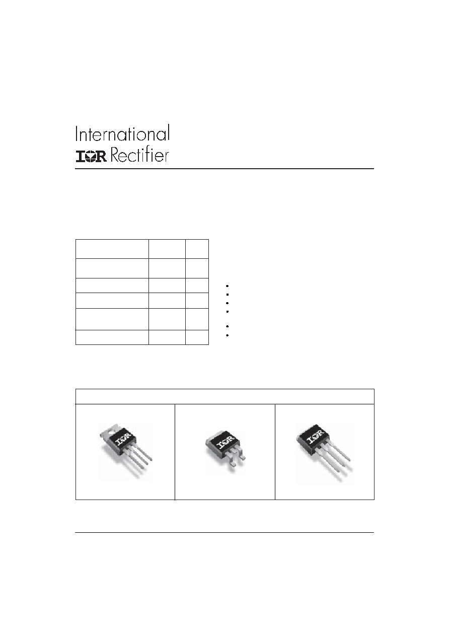
Description/ Features
Case Styles
16CTQ...-1
TO-220
D
2
PAK
TO-262
16CTQ...
16CTQ...S
16CTQ...-1
Major Ratings and Characteristics
I
F(AV)
Rectangular
16
A
waveform
V
RRM
60 / 100
V
I
FSM
@ tp = 5 µs sine
850
A
V
F
@
8 Apk, T
J
= 125∞C
0.58
V
(per leg)
T
J
range
- 55 to 175
∞C
Characteristics
Values
Units
16CTQ...
16CTQ...S
16CTQ..., 16CTQ...S, 16CTQ...-1
2
Bulletin PD-20192 rev. H 12/03
www.irf.com
16CTQ060
16CTQ80
16CTQ100
16CTQ060S
16CTQ80S
16CTQ100S
16CTQ060-1
16CTQ80-1
16CTQ100-1
V
R
Max. DC Reverse Voltage (V)
V
RWM
Max. Working Peak Reverse Voltage (V)
60
80
100
Voltage Ratings
Parameters
Absolute Maximum Ratings
Parameters
Values Units
Conditions
I
F(AV)
Max. Average Forward
(Per Leg)
8
A
50% duty cycle @ T
C
= 148∞C, rectangular wave form
Current
* See Fig. 5
(Per Device)
16
I
FSM
Max. Peak One Cycle Non-Repetitive
850
5µs Sine or 3µs Rect. pulse
Surge Current (Per Leg) * See Fig. 7
275
10ms Sine or 6ms Rect. pulse
E
AS
Non-Repetitive Avalanche Energy
7.50
mJ
T
J
= 25 ∞C, I
AS
= 0.50 Amps, L = 60 mH
(Per Leg)
I
AR
Repetitive Avalanche Current
0.50
A
Current decaying linearly to zero in 1 µsec
(Per Leg)
Frequency limited by T
J
max. V
A
= 1.5 x V
R
typical
A
T
J
Max. Junction Temperature Range
-55 to 175
∞C
T
stg
Max. Storage Temperature Range
-55 to 175
∞C
R
thJC
Max. Thermal Resistance Junction
3.25
∞C/W DC operation
to Case (Per Leg)
R
thJC
Max. Thermal Resistance Junction
1.63
∞C/W DC operation
to Case (Per Package)
R
thCS
Typical Thermal Resistance, Case
0.50
∞C/W Mounting surface , smooth and greased
to Heatsink (only for TO-220)
wt
Approximate Weight
2 (0.07)
g (oz.)
T
Mounting Torque
Min.
6 (5)
Max.
12 (10)
Thermal-Mechanical Specifications
Kg-cm
(Ibf-in)
Parameters
Values Units
Conditions
V
FM
Max. Forward Voltage Drop
0.72
V
@ 8A
(Per Leg) * See Fig. 1
(1)
0.88
V
@ 16A
0.58
V
@ 8A
0.69
V
@ 16A
I
RM
Max. Reverse Leakage Current
0.55
mA
T
J
= 25 ∞C
(Per Leg) * See Fig. 2
(1)
7.0
mA
T
J
= 125 ∞C
V
F(TO)
Threshold Voltage
0.415
V
T
J
= T
J
max.
r
t
Forward Slope Resistance
11.07
m
C
T
Max. Junction Capacitance (Per Leg)
500
pF
V
R
= 5V
DC
, (test signal range 100Khz to 1Mhz) 25∞C
L
S
Typical Series Inductance (Per Leg)
8.0
nH
Measured lead to lead 5mm from package body
dv/dt Max. Voltage Rate of Change
10,000
V/ µs
(Rated V
R
)
T
J
= 25 ∞C
T
J
= 125 ∞C
Electrical Specifications
(1) Pulse Width < 300µs, Duty Cycle <2%
V
R
= rated V
R
Parameters
Values Units
Conditions
Following any rated
load condition and with
rated V
RRM
applied
3
Bulletin PD-20192 rev. H 12/03
www.irf.com
16CTQ..., 16CTQ...S, 16CTQ...-1
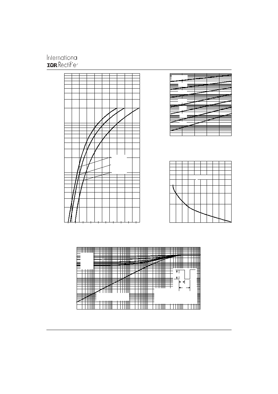
Fig. 2 - Typical Values Of Reverse Current
Vs. Reverse Voltage (Per Leg)
Fig. 3 - Typical Junction Capacitance
Vs. Reverse Voltage (Per Leg)
Fig. 4 - Max. Thermal Impedance Z
thJC
Characteristics (Per Leg)
Fig. 1 - Max. Forward Voltage Drop Characteristics
(Per Leg)
1
10
100
1000
0.2 0.4 0.6 0.8
1
1.2 1.4 1.6 1.8
2
2.2
I
n
s
t
a
n
t
a
n
e
o
u
s
F
o
rw
a
r
d
C
u
rre
n
t
-
I
(
A
)
F
FM
Forward Voltage Drop - V (V)
T = 175∞C
T = 125∞C
T = 25∞C
J
J
J
0.0001
0.001
0.01
0.1
1
10
100
0
20
40
60
80
100
R
R
150∞C
125∞C
100∞C
75∞C
50∞C
25∞C
R
e
v
e
rs
e
C
u
r
r
e
n
t
-
I
(m
A
)
T = 175∞C
J
Reverse Voltage - V (V)
100
1000
0
20
40
60
80
100
T = 25∞C
J
R
J
u
n
c
t
i
o
n
C
apac
i
t
an
c
e
-
C
(
p
F
)
T
Reverse Voltage - V (V)
0.001
0.01
0.1
1
10
0.00001
0.0001
0.001
0.01
0.1
1
10
100
th
J
C
t , Rectangular Pulse Duration (Seconds)
Single Pulse
(Thermal Resistance)
1
T
h
e
r
m
a
l
I
m
pedan
c
e
Z
(
∞
C
/
W
)
D = 0.75
D = 0.50
D = 0.33
D = 0.25
D = 0.20
J
DM
thJC
C
2
t
1
t
P
DM
1
2
Notes:
1. Duty factor D = t / t
2. Peak T = P x Z + T
16CTQ..., 16CTQ...S, 16CTQ...-1
4
Bulletin PD-20192 rev. H 12/03
www.irf.com
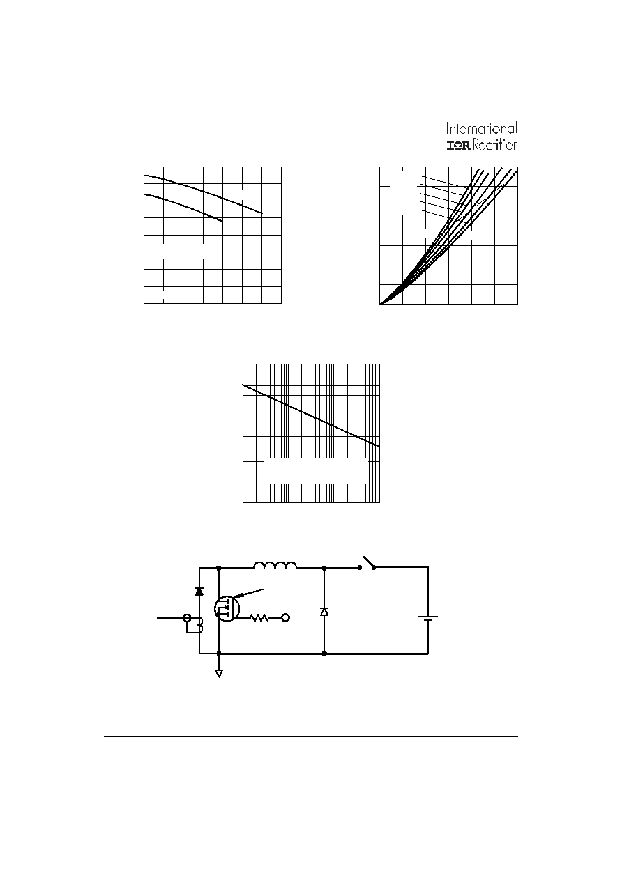
Fig. 8 - Unclamped Inductive Test Circuit
FREE-WHEEL
DIODE
40HFL40S02
CURRENT
MONITOR
HIGH-SPEED
SWITCH
IRFP460
L
DUT
Rg = 25 ohm
Vd = 25 Volt
+
(2) Formula used: T
C
= T
J
- (Pd + Pd
REV
) x R
thJC
;
Pd = Forward Power Loss = I
F(AV)
x V
FM
@ (I
F(AV)
/
D) (see Fig. 6);
Pd
REV
= Inverse Power Loss = V
R1
x I
R
(1 - D); I
R
@ V
R1
= 10 V
Fig. 7 - Max. Non-Repetitive Surge Current (Per Leg)
Fig. 5 - Max. Allowable Case Temperature
Vs. Average Forward Current (Per Leg)
Fig. 6 - Forward Power Loss Characteristics
(Per Leg)
100
110
120
130
140
150
160
170
180
0
2
4
6
8
10
12
14
DC
A
l
l
o
w
a
b
l
e
C
a
s
e
T
e
m
p
e
r
at
u
r
e -
(
∞
C
)
F(AV)
see note (2)
Squa re wave (D = 0.50)
80% Ra ted V a pplied
R
Average Forward Current - I (A)
0
1
2
3
4
5
6
7
0
2
4
6
8
10
12
DC
A
v
er
ag
e
P
o
w
e
r
L
o
s
s
-
(
W
a
t
t
s
)
F(AV)
RMS Limit
D = 0.20
D = 0.25
D = 0.33
D = 0.50
D = 0.75
Average Forward Current - I (A)
100
1000
10
100
1000
10000
FS
M
N
o
n
-
R
e
p
e
t
i
t
i
v
e
S
u
rg
e
C
u
rre
n
t
- I
(
A
)
p
At Any Rated Load Condition
And With Rated V Applied
Following Surge
RRM
Square Wave Pulse Duration - t (microsec)
5
Bulletin PD-20192 rev. H 12/03
www.irf.com
16CTQ..., 16CTQ...S, 16CTQ...-1
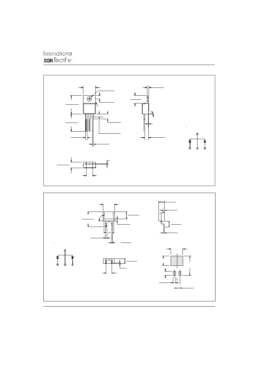
3.78 (0.15)
3.54 (0.14)
10.54 (0.41)
MAX.
DIA.
15.24 (0.60)
14.84 (0.58)
2.92 (0.11)
2.54 (0.10)
1
TERM 2
14.09 (0.55)
13.47 (0.53)
3.96 (0.16)
3.55 (0.14)
0.94 (0.04)
0.69 (0.03)
4.57 (0.18)
4.32 (0.17)
3
0.61 (0.02) MAX.
5.08 (0.20) REF.
1.32 (0.05)
1.22 (0.05)
6.48 (0.25)
6.23 (0.24)
2∞
0.10 (0.004)
1.40 (0.05)
1.15 (0.04)
2.89 (0.11)
2.64 (0.10)
1
3
2.04 (0.080) MAX.
2
2
Conform to JEDEC outline TO-220AB
Dimensions in millimeters and (inches)
2
BASE
COMMON
CATHODE
1
2
3
ANODE
COMMON
CATHODE
ANODE
1
2
Outline Table
10.16 (0.40)
REF.
8.89 (0.35)
4.57 (0.18)
4.32 (0.17)
0.61 (0.02) MAX.
5.08 (0.20) REF.
1.32 (0.05)
1.22 (0.05)
1
3
6.47 (0.25)
6.18 (0.24)
93∞
REF.
2.61 (0.10)
2.32 (0.09)
5.28 (0.21)
4.78 (0.19)
4.69 (0.18)
4.20 (0.16)
0.55 (0.02)
0.46 (0.02)
14.73 (0.58)
15.49 (0.61)
1.40 (0.055)
1.14 (0.045)
3X
0.93 (0.37)
0.69 (0.27)
2X
11.43 (0.45)
17.78 (0.70)
8.89 (0.35)
3.81 (0.15)
2.08 (0.08)
2X
2.54 (0.10)
2X
MINIMUM RECOMMENDED FOOTPRINT
2
Conform to JEDEC outline D
2
Pak (SMD-220)
Dimensions in millimeters and (inches)
2
BASE
COMMON
CATHODE
1
2
3
ANODE
COMMON
CATHODE
ANODE
1
2