1
25MT060WF
Target Data 05/01
V
CES
= 600V
V
CE(on) typ.
= 2.2V @
V
GE
= 15V, I
C
= 25A
T
C
= 25°C
Absolute Maximum Ratings
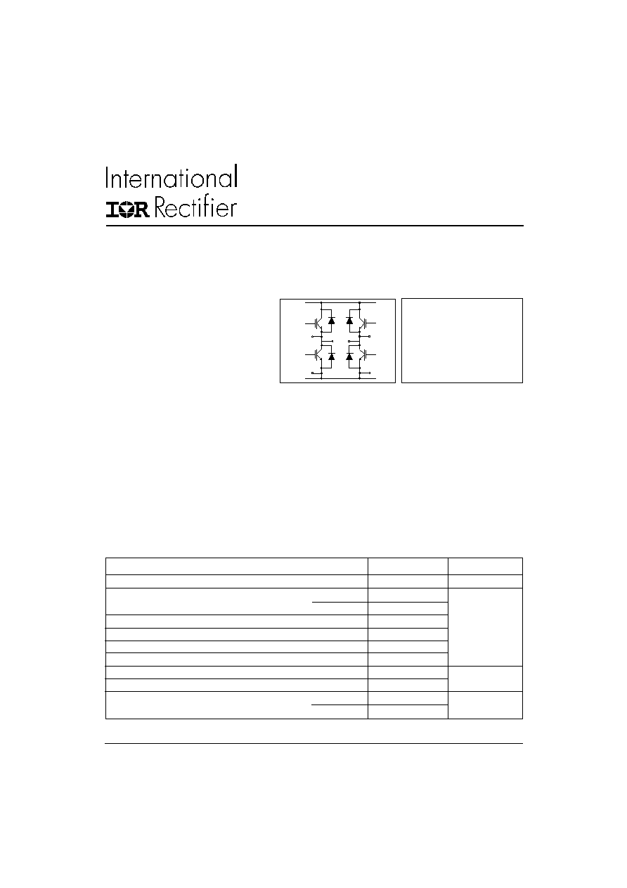
"FULL-BRIDGE" IGBT MTP
V
CES
Collector-to-Emitter Voltage
600
V
I
C
Continuos Collector Current
@ T
C
= 25°C
50
A
@ T
C
= 100°C
25
I
CM
Pulsed Collector Current
200
I
LM
Peak Switching Current
200
I
F
Diode Continuous Forward Current
@ T
C
= 100°C
25
I
FM
Peak Diode Forward Current
200
V
GE
Gate-to-Emitter Voltage
± 20
V
V
ISOL
RMS Isolation Voltage, Any Terminal to Case, t = 1 min
2500
P
D
Maximum Power Dissipation
@ T
C
= 25°C
900
W
@ T
C
= 100°C
400
Parameters
Max
Units
Warp Speed IGBT
· Gen. 4 Warp Speed IGBT Technology
· HEXFRED
TM
Antiparallel Diodes with
UltraSoft Reverse Recovery
· Very Low Conduction and Switching Losses
· Optional SMT Thermystor Inside
· Aluminum Nitride DBC
· Very Low Stray Inductance Design for
High Speed Operation
Features
· Optimized for Welding, UPS and SMPS Applications
· Operating Frequencies > 20 kHz Hard Switching,
>200 kHz Resonant Mode
· Low EMI, requires Less Snubbing
· Direct Mounting to Heatsink
· PCB Solderable Terminals
· Very Low Junction-to-Case Thermal Resistance
Benefits
25MT060WF
Target Data 05/01
2
V
(BR)CES
Collector-to-Emitter Breakdown Voltage
600
V
V
GE
= 0V, I
C
= 250µA
V
CE(on)
Collector-to-Emitter Voltage
1.85
V
GE
= 15V, I
C
= 25A
1.7
V
GE
= 15V, I
C
= 25A, T
J
= 150°C
V
GE(th)
Gate Threshold Voltage
3
6
I
C
= 250µA
V
GE(th)
/ Temperature Coeff. of
-
mV/°C V
GE
= V
CE
, I
C
= 500µA
T
J
Threshold Voltage
g
fe
Forward Transconductance
40
S
V
CE
= 100V, I
C
= 25A
I
CES
Collector-to-Emiter Leaking Current
250
µA
V
GE
= 0V, V
CE
= 600V
5000
V
GE
= 0V, V
CE
= 600V, T
J
= 150°C
V
F M
Diode Forward Voltage Drop
1.3
V
I
F
= 25A, V
GE
= 0V
1.2
I
F
= 25A, V
GE
= 0V, T
J
= 150°C
I
GES
Gate-to-Emitter Leakage Current
± 100
nA
V
GE
= ± 20V
Electrical Characteristics @ T
J
= 25°C (unless otherwise specified)
Parameters
Min Typ Max Units Test Conditions
Thermal- Mechanical Specifications
T
J
Operating Junction Temperature Range
- 40
150
°C
T
STG
Storage Temperature Range
- 40
125
R
thJC
Junction-to-Case
IGBT
0.7
°C/ W
Diode
0.9
R
thCS
Case-to-Sink
Module
0.06
(Heatsink Compound Thermal Conductivity = 1 W/mK)
Weight
66
g
Parameters
Min
Typ
Max
Units
Q
g
Total Gate Charge (turn-on)
180
nC
I
C
= 25A
Q
ge
Gate-Emitter Charge (turn-on)
25
V
CC
= 400V
Q
gc
Gate-Collector Charge (turn-on)
63
V
GE
= 15V
E
on
Turn-On Switching Loss
950
µJ
R
g1
= R
g2
= 5
,
I
C
= 25A
E
off(1)
Turn-Off Switching Loss
320
V
CC
= 480V
E
ts(1)
Total Switching Loss
1270
V
GE
= ±15V
C
ies
Input Capacitance
4000
pF
V
GE
= 0V
C
oes
Output Capacitance
260
V
CC
= 30V
C
res
Reverse Transfer Capacitance
68
f = 1.0 MHz
trr
Diode Reverse Recovery Time
50
ns
V
R
= 200V, I
C
= 25A
Irr
Diode Peak Reverse Current
4.5
A
di/dt = 200A/µs
Qrr
Diode Recovery Charge
112
nC
di
(rec)
M/
dt
Diode PeakRate of Fall of Recovery
250
A/µs
During t
b
Switching Characteristics @ T
J
= 25°C (unless otherwise specified)
Parameters
Min Typ Max Units Test Conditions
Target Data 05/01
3
25MT060WF
IR WORLD HEADQUARTERS: 233 Kansas St., El Segundo, California 90245, USA Tel: (310) 252-7105
TAC Fax: (310) 252-7309
Visit us at www.irf.com for sales contact information. 05/01
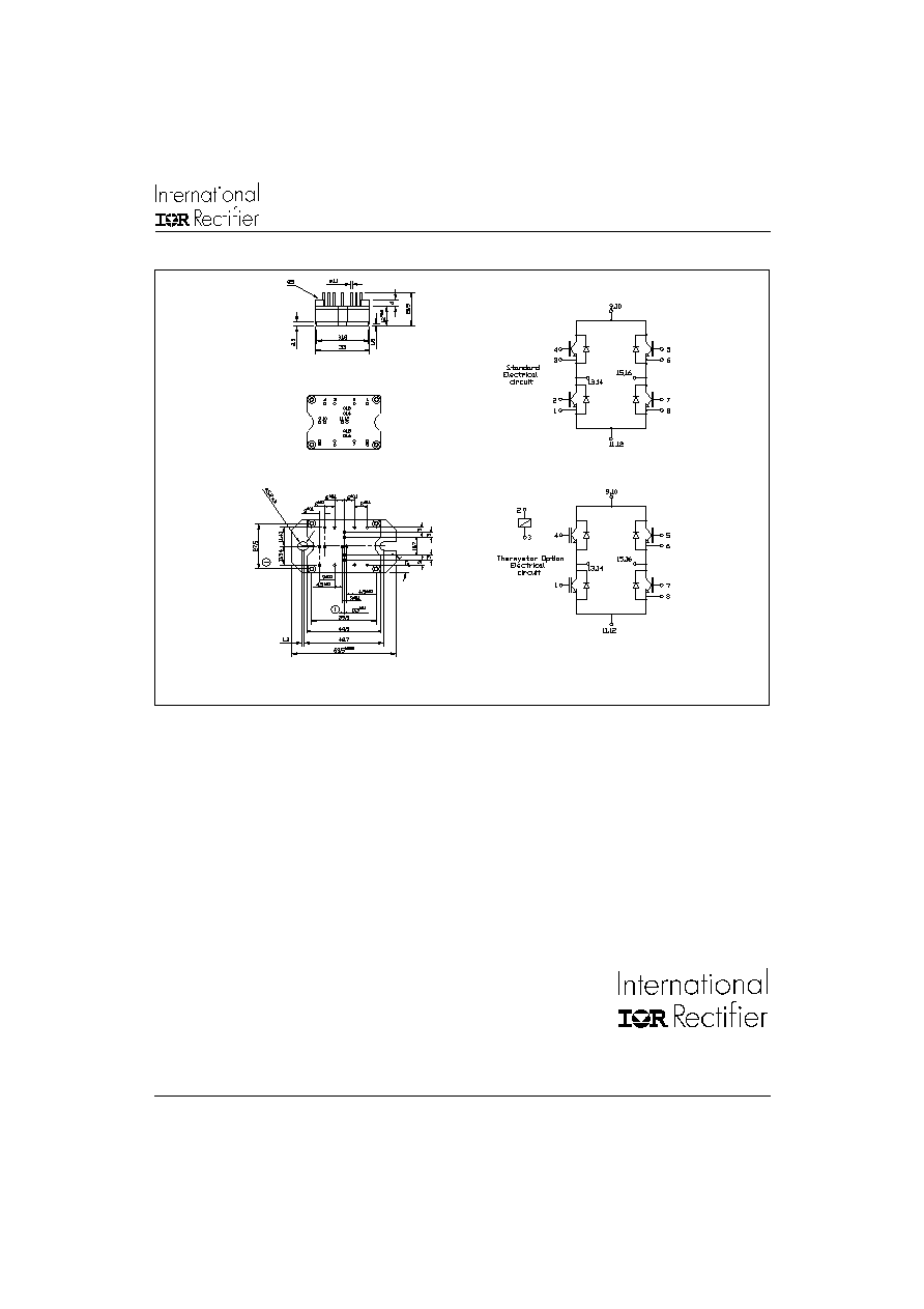
Outline Table
Data and specifications subject to change without notice.
This product has been designed for Industrial Level.
Qualification Standards can be found on IR's Web site.
Dimensions in millimeters