 | –≠–ª–µ–∫—Ç—Ä–æ–Ω–Ω—ã–π –∫–æ–º–ø–æ–Ω–µ–Ω—Ç: 25TTS08 | –°–∫–∞—á–∞—Ç—å:  PDF PDF  ZIP ZIP |
1
PHASE CONTROL SCR
TO-220 FULLPAK
Bulletin I2135 rev. D 03/99
SAFE
IR
Series
25TTS..FP
V
T
< 1.25V @ 16A
I
TSM
= 300A
V
RRM
800 to 1600V
www.irf.com
Description/Features
The 25TTS..FP
SAFE
IR
series of silicon
controlled rectifiers are specifically designed for
medium power switching and phase control
applications. The glass passivation technology
used has reliable operation up to 125∞ C junction
temperature.
Typical applications are in input rectification (soft
start) and these products are designed to be used
with International Rectifier input diodes, switches
and output rectifiers which are available in identical
package outlines.
Fully isolated package (V
INS
= 2500 V
RMS
)
UL E78996 approved
Major Ratings and Characteristics
TO-220 FULLPAK
Capacitive input filter T
A
= 55∞C, T
J
= 125∞C,
18
22
A
common heatsink of 1∞C/W
Output Current in Typical Applications
Applications
Single-phase Bridge
Three-phase Bridge
Units
I
T(AV)
Sinusoidal
16
A
waveform
I
RMS
25
A
V
RRM
/ V
DRM
up to 1600
V
I
TSM
300
A
V
T
@ 16 A, T
J
= 25∞C
1.25
V
dv/dt
500
V/µs
di/dt
150
A/µs
T
J
- 40 to 125
∞C
Characteristics
25TTS..FP Units
Package Outline
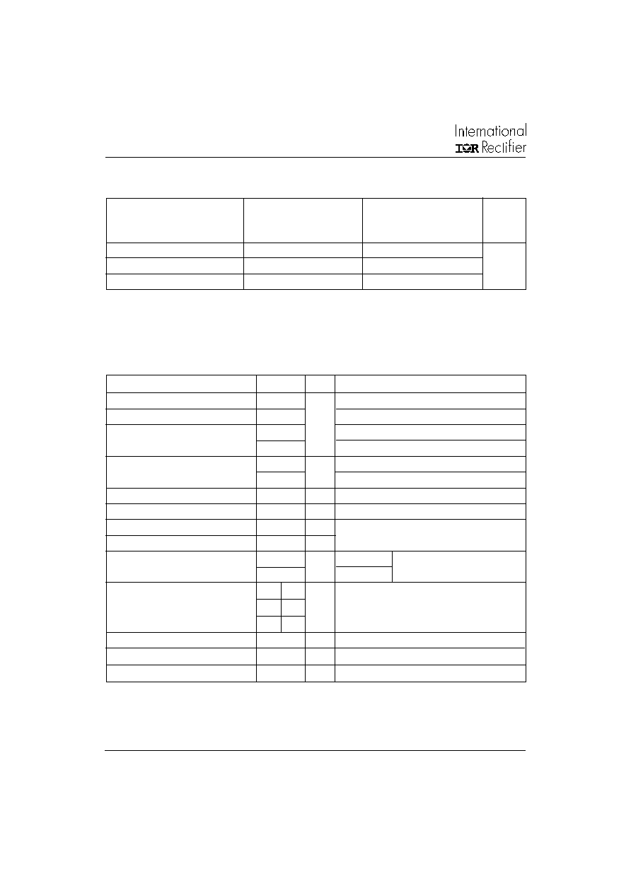
2
25TTS..FP
SAFE
IR
Series
Bulletin I2135 rev. D 03/99
www.irf.com
Part Number
V
RRM
, maximum
V
DRM
, maximum
I
RRM
/
I
DRM
peak reverse voltage
peak direct voltage
125∞C
V
V
mA
25TTS08FP
800
800
10
25TTS12FP
1200
1200
25TTS16FP
1600
1600
Voltage Ratings
I
T(AV)
Max. Average On-state Current
16
A
@ T
C
= 85∞ C, 180∞ conduction half sine wave
I
RMS
Max. RMS On-state Current
25
I
TSM
Max. Peak One Cycle Non-Repetitive
300
10ms Sine pulse, rated V
RRM
applied
Surge Current
350
10ms Sine pulse, no voltage reapplied
I
2
t
Max. I
2
t for fusing
450
A
2
s
10ms Sine pulse, rated V
RRM
applied
630
10ms Sine pulse, no voltage reapplied
I
2
t
Max. I
2
t for fusing
6300
A
2
s
t = 0.1 to 10ms, no voltage reapplied
V
TM
Max. On-state Voltage Drop
1.25
V
@ 16A, T
J
= 25∞C
r
t
On-state slope resistance
12.0
m
T
J
= 125∞C
V
T(TO)
Threshold Voltage
1.0
V
I
RM
/I
DM
Max.Reverse and Direct
0.5
mA
T
J
= 25 ∞C
Leakage Current
10
T
J
= 125 ∞C
I
H
Holding Current
Typ.
Max.
Anode Supply = 6V, Resistive load, Initial I
T
=1A
--
100
mA
25TTS08FP, 25TTS12FP
100
150
25TTS16FP
I
L
Max. Latching Current
200
mA
Anode Supply = 6V, Resistive load
dv/dt Max. Rate of Rise of off-state Voltage
500
V/µs
di/dt Max. Rate of Rise of turned-on Current
150
A/µs
Absolute Maximum Ratings
Parameters
25TTS..FP Units
Conditions
V
R
= rated V
RRM
/ V
DRM
3
25TTS..FP
SAFE
IR
Series
Bulletin I2135 rev. D 03/99
www.irf.com
Triggering
P
GM
Max. peak Gate Power
8.0
W
P
G(AV)
Max. average Gate Power
2.0
+ I
GM
Max. paek positive Gate Current
1.5
A
- V
GM
Max. paek negative Gate Voltage
10
V
I
GT
Max. required DC Gate Current
60
mA
Anode supply = 6V, resistive load, T
J
= - 10∞C
to trigger
45
Anode supply = 6V, resistive load, T
J
= 25∞C
20
Anode supply = 6V, resistive load, T
J
= 125∞C
V
GT
Max. required DC Gate Voltage
2.5
V
Anode supply = 6V, resistive load, T
J
= - 10∞C
to trigger
2.0
Anode supply = 6V, resistive load, T
J
= 25∞C
1.0
Anode supply = 6V, resistive load, T
J
= 125∞C
V
GD
Max. DC Gate Voltage not to trigger
0.25
T
J
= 125∞C, V
DRM
= rated value
I
GD
Max. DC Gate Current not to trigger
2.0
mA
T
J
= 125∞C, V
DRM
= rated value
Parameters
25TTS..FP Units
Conditions
Switching
Parameters
25TTS..FP Units
Conditions
t
gt
Typical turn-on time
0.9
µs
T
J
= 25∞C
t
rr
Typical reverse recovery time
4
T
J
= 125∞C
t
q
Typical turn-off time
110
T
J
Max. Junction Temperature Range
- 40 to 125
∞C
T
stg
Max. Storage Temperature Range
- 40 to 125
R
thJC
Max. Thermal Resistance Junction
1.5
∞C/W
DC operation
to Case
R
thJA
Max. Thermal Resistance Junction
62
to Ambient
R
thCS
Typ. Thermal Resistance Case
1.5
Mounting surface, smooth and greased
to Heatsink
wt
Approximate Weight
2 (0.07)
g (oz.)
T
Mounting Torque
Min.
6 (5)
Max.
12 (10)
Case Style
TO-220 FULLPAK
(94/V0)
Thermal-Mechanical Specifications
Parameters
25TTS..FP Units
Conditions
Kg-cm
(Ibf-in)
4
25TTS..FP
SAFE
IR
Series
Bulletin I2135 rev. D 03/99
www.irf.com
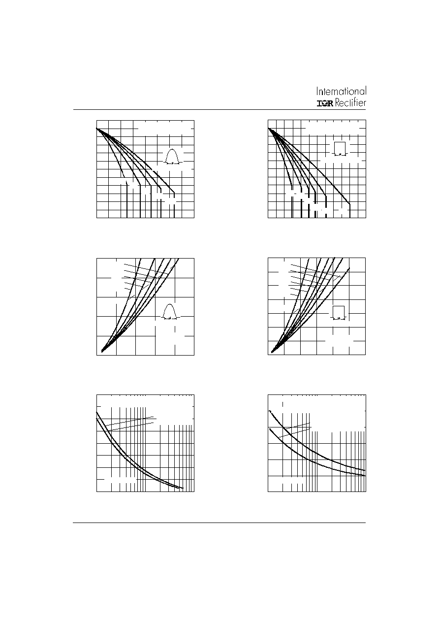
Fig. 1 - Current Rating Characteristics
Fig. 2 - Current Rating Characteristics
Fig. 3 - On-state Power Loss Characteristics
Fig. 4 - On-state Power Loss Characteristics
Fig. 5 - Maximum Non-Repetitive Surge Current
Fig. 6 - Maximum Non-Repetitive Surge Current
0
5
10
15
20
25
0
4
8
12
16
20
RMS Limit
Conduction Angle
M
a
x
i
mu
m
A
v
e
r
a
g
e
O
n
-
s
t
a
t
e
P
o
w
e
r
Lo
s
s
(
W
)
Average On-state Current (A)
180∞
120∞
90∞
60∞
30∞
25TTS.. Series
T = 125∞C
J
0
5
10
15
20
25
30
35
0
5
10
15
20
25
30
DC
180∞
120∞
90∞
60∞
30∞
RMS Limit
Conduction Period
M
a
x
i
mu
m A
v
e
r
a
g
e
O
n
-
s
t
a
t
e
P
o
w
e
r
L
o
ss (
W
)
Average On-state Current (A)
25TTS.. Series
T = 125∞C
J
150
200
250
300
350
1
10
100
Number Of Equal Amplitude Half Cycle Current Pulses (N)
P
e
ak
Ha
l
f
S
i
n
e
W
a
v
e
O
n
-
s
t
a
t
e
C
u
r
r
e
n
t
(A
)
Initial T = 125∞C
@ 60 Hz 0.0083 s
@ 50 Hz 0.0100 s
J
25TTS.. Series
At Any Rated Load Condition And With
Rated V Applied Following Surge.
RRM
100
150
200
250
300
350
400
0.01
0.1
1
P
e
ak
Hal
f
S
i
ne
W
a
v
e
O
n
-
s
t
a
t
e
C
u
r
r
e
nt
(A
)
Pulse Train Duration (s)
Maximum Non Repetitive Surge Current
Versus Pulse Train Duration. Control
Of Conduction May Not Be Maintained.
Initial T = 125∞C
No Voltage Reapplied
Rated V Reapplied
RRM
J
25TTS.. Series
70
80
90
100
110
120
130
0
5
10
15
20
30∞
60∞
90∞
120∞
180∞
M
a
x
i
m
u
m
A
l
l
o
w
a
b
l
e C
a
s
e
Tem
p
er
a
t
u
r
e (
∞C
)
Conduction Angle
Average On-state Current (A)
25TTS.. Series
R (DC) = 1.5 ∞C/W
thJC
70
80
90
100
110
120
130
0
5
10
15
20
25
30
DC
30∞
60∞
90∞
120∞
180∞
M
a
x
i
m
u
m
A
l
l
o
w
a
b
l
e
C
a
s
e
Tem
p
e
r
a
t
u
r
e
(
∞C
)
Conduction Period
Average On-state Current (A)
25TTS.. Series
R (DC) = 1.5 ∞C/W
thJC
5
25TTS..FP
SAFE
IR
Series
Bulletin I2135 rev. D 03/99
www.irf.com
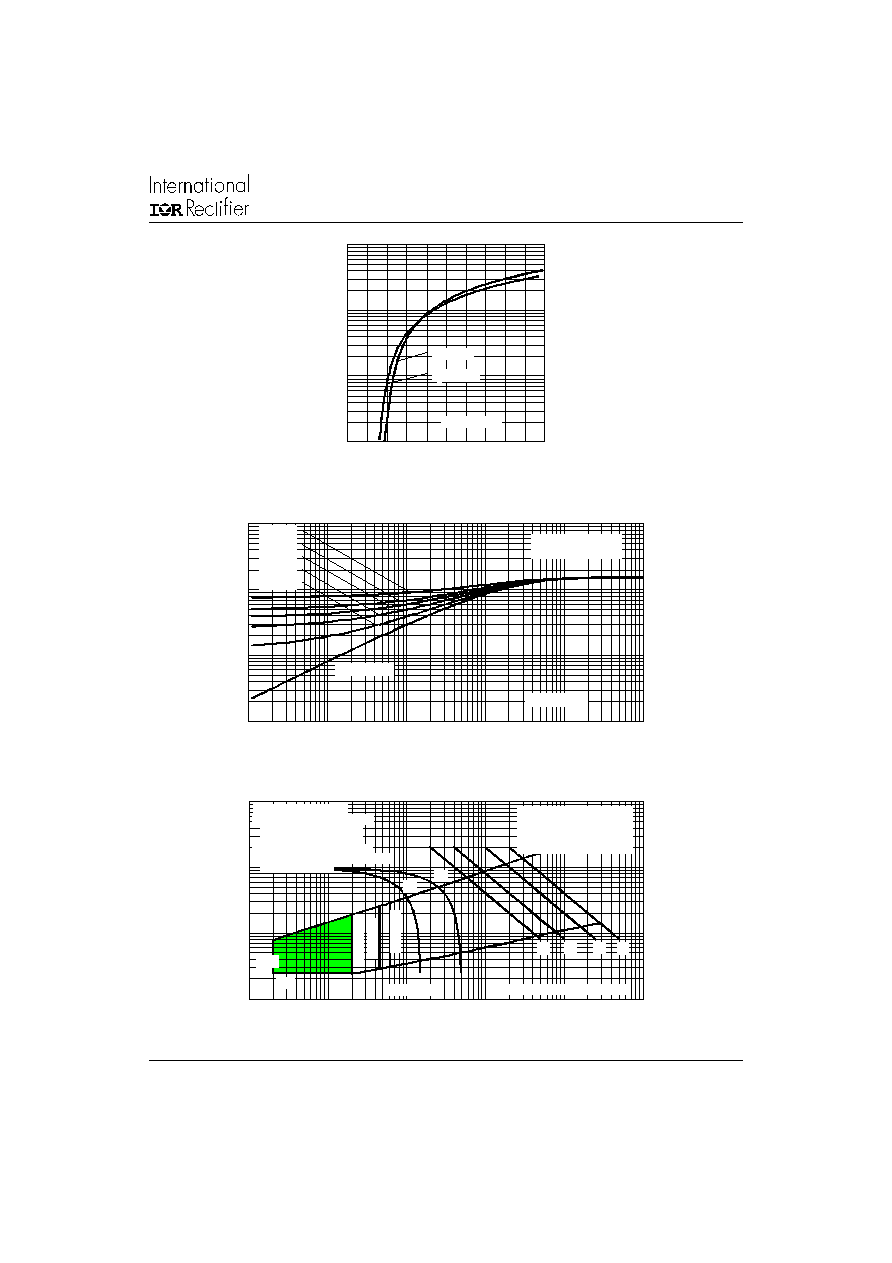
Fig. 7 - On-state Voltage Drop Characteristics
Fig. 9 - Gate Characteristics
Fig. 8 - Thermal Impedance Z
thJC
Characteristics
1
10
100
1000
0
1
2
3
4
5
T = 25∞C
J
I
n
s
t
a
n
ta
n
e
ou
s
O
n
-
s
ta
t
e
Cu
r
r
e
n
t
(
A
)
Instantaneous On-state Voltage (V)
T = 125∞C
J
25TTS.. Series
0.1
1
10
100
0.001
0.01
0.1
1
10
100
(b)
(a)
Rectangular gate pulse
(4)
(3)
(2)
(1)
Instantaneous Gate Current (A)
I
n
s
t
a
n
ta
n
e
o
u
s
G
a
te
V
o
l
t
a
g
e
(
V
)
TJ
=
2
5
∞C
T
J
=
125 ∞
C
b)Recommended load line for
Frequency Limited by PG(AV)
a)Recommended load line for
rated di/dt: 10 V, 20 ohms
tr = 0.5 µs, tp >= 6 µs
TJ
=
-
1
0
∞C
25TTS.. Series
IGD
VGD
<= 30% rated di/dt: 10 V, 65 ohms
tr = 1 µs, tp >= 6 µs
(1) PGM = 40 W, tp = 1 ms
(2) PGM = 20 W, tp = 2 ms
(3) PGM = 8 W, tp = 5 ms
(4) PGM = 4 W, tp = 10 ms
0.01
0.1
1
10
0. 0001
0.001
0.01
0.1
1
10
Square Wave Pulse Duration (s)
D = 0.50
D = 0.33
D = 0.25
D = 0.17
D = 0.08
Steady State Value
(DC Operation)
25TTS.. Series
th
J
C
Single Pulse
T
r
a
n
s
i
en
t
T
h
er
m
a
l
I
m
p
e
d
a
n
c
e
Z
(
∞C
/
W
)