 | –≠–ª–µ–∫—Ç—Ä–æ–Ω–Ω—ã–π –∫–æ–º–ø–æ–Ω–µ–Ω—Ç: 32CTQ030S | –°–∫–∞—á–∞—Ç—å:  PDF PDF  ZIP ZIP |
SCHOTTKY RECTIFIER
32 Amp
32CTQ030
32CTQ030S
32CTQ030-1
Bulletin PD-20265 07/00
Major Ratings and Characteristics
I
F(AV)
Rectangular
30
A
waveform
V
RRM
30
V
I
FSM
@ tp = 5 µs sine
900
A
V
F
@
15 Apk, T
J
= 125∞C
0.40
V
T
J
range
- 55 to 150
∞C
Characteristics
32CTQ
Units
Description/Features
The 32CTQ030 Schottky rectifier series has been optimized
for low reverse leakage at high temperature. The proprietary
barrier technology allows for reliable operation up to 150∞ C
junction temperature. Typical applications are in switching
power supplies, converters, free-wheeling diodes, and re-
verse battery protection.
150∞ C T
J
operation
High purity, high temperature epoxy encapsulation for
enhanced mechanical strength and moisture resistance
Low forward voltage drop
High frequency operation
Guard ring for enhanced ruggedness and long term
reliability
1
I
F(AV)
= 30Amp
V
R
= 30V
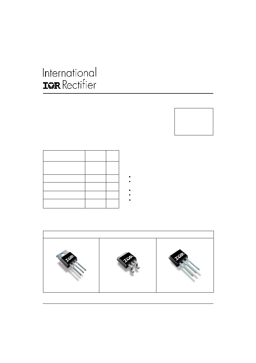
Case Styles
32CTQ030
32CTQ030S
32CTQ030-1
TO-220
D
2
PAK
TO-262

32CTQ030, 32CTQ030S, 32CTQ030-1
2
Bulletin PD-20265 07/00
www.irf.com
V
FM
Max. Forward Voltage Drop (1)
0.49
V
@ 15A
* See Fig. 1
0.58
V
@ 30A
0.40
V
@ 15A
0.53
V
@ 30A
I
RM
Max. Reverse Leakage Current (1)
1.75
mA
T
J
= 25 ∞C
* See Fig. 2
97
mA
T
J
= 125 ∞C
V
F(TO)
Threshold Voltage
0.233
V
T
J
= T
J
max.
r
t
Forward Slope Resistance
9.09
m
C
T
Max. Junction Capacitance Per Leg
1300
pF
V
R
= 5V
DC
, (test signal range 100Khz to 1Mhz) 25 ∞C
L
S
Typical Series Inductance
Per Leg
8.0
nH
Measured lead to lead 5mm from package body
dv/dt Max. Voltage Rate of Change
10,000
V/ µs
(Rated V
R
)
T
J
= 25 ∞C
T
J
= 125 ∞C
V
R
= rated V
R
Electrical Specifications
(1) Pulse Width < 300µs, Duty Cycle < 2%
T
J
Max. Junction Temperature Range
- 55 to 150
∞C
T
stg
Max. Storage Temperature Range
- 55 to 150
∞C
R
thJC
Max. Thermal Resistance Junction
3.25
∞C/W
DC operation
* See Fig. 4
to Case
Per Leg
R
thCS
Typical Thermal Resistance,
0.50
∞C/W
Mounting surface , smooth and greased
Case to Heatsink
wt
Approximate Weight
2 (0.07) g (oz.)
T
Mounting Torque
Min.
6 (5)
Max.
12 (10)
Kg-cm
(Ibf-in)
Thermal-Mechanical Specifications
Part number
32CTQ030
V
R
Max. DC Reverse Voltage (V)
V
RWM
Max. Working Peak Reverse Voltage (V)
30
Voltage Ratings
I
F(AV)
Max. Average Forward Current
30
A
50% duty cycle @ T
C
= 115∞ C, rectangular wave form
* See Fig. 5
I
FSM
Max. Peak One Cycle Non-Repetitive
900
5µs Sine or 3µs Rect. pulse
Surge Current * See Fig. 7
250
10ms Sine or 6ms Rect. pulse
E
AS
Non-Repetitive Avalanche Energy
13
mJ
T
J
= 25 ∞C, I
AS
= 1.20 Amps, L = 11.10 mH
I
AR
Repetitive Avalanche Current
3
A
Current decaying linearly to zero in 1 µsec
Frequency limited by T
J
max. V
A
= 1.5 x V
R
typical
Parameters
32CTQ Units Conditions
Absolute Maximum Ratings
A
Following any rated
load condition and
with rated V
RRM
applied
Parameters
32CTQ Units Conditions
Parameters
32CTQ Units Conditions

32CTQ030, 32CTQ030S, 32CTQ030-1
3
Bulletin PD-20265 07/00
www.irf.com
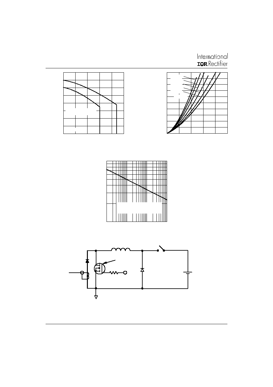
Fig. 2 - Typical Values of Reverse Current
Vs. Reverse Voltage
Fig. 3 - Typical Junction Capacitance
Vs. Reverse Voltage
Fig. 4 - Maximum Thermal Impedance Z
thJC
Characteristics
Fig. 1 - Maximum Forward Voltage Drop Characteristics
1
10
1 00
10 0 0
0
0 .2
0.4
0.6
0 .8
1
1.2
1.4
1.6
1 .8
I
n
s
t
an
t
a
n
e
o
u
s
F
o
r
w
ar
d C
u
r
r
e
n
t
-
I
(
A
)
T = 150 C
T = 125 C
T = 25 C
J
J
J
F
FM
Forw a rd V olta g e D rop - V (V )
0 .00 1
0.0 1
0 .1
1
10
10 0
10 0 0
0
5
1 0
1 5
2 0
2 5
30
R
R
125 C
100 C
75 C
50 C
25 C
Re
v
e
r
s
e
C
u
r
r
e
n
t
-
I
(
m
A
)
T = 150 C
J
Re ve rse V oltag e - V (V )
1 00
1 0 00
1 00 00
0
5
1 0
1 5
2 0
2 5
3 0
35
R
T
J
u
n
c
ti
on
C
a
pa
c
i
tan
c
e
-
C
(
p
F)
Re ve rse V olta g e - V (V )
T = 25 C
J
0 .0 01
0. 01
0 .1
1
1 0
0 .0 0 0 01
0 .0 00 1
0 .0 0 1
0 .0 1
0. 1
1
1 0
th
J
C
t , Recta ngula r Pulse Dura tio n (Seco nd s)
Sin g le Pu lse
(Therm a l Resista nce)
1
T
h
e
r
m
a
l
I
m
p
e
d
a
n
c
e
Z
(
C
/
W
)
D = 0.75
D = 0.50
D = 0.33
D = 0.25
D = 0.2 0
J
D M
th J C
C
2
t
1
t
P
D M
1
2
N o te s:
1. D uty fa c to r D = t / t
2. P e ak T = P x Z + T
32CTQ030, 32CTQ030S, 32CTQ030-1
4
Bulletin PD-20265 07/00
www.irf.com
Fig. 8 - Unclamped Inductive Test Circuit
Fig. 5 - Maximum Allowable Case Temperature
Vs. Average Forward Current
Fig. 6 - Forward Power Loss Characteristics
Fig. 7 - Maximum Non-Repetitive Surge Current
FR EE-W HE EL
D IO D E
40H FL40S02
C UR RE N T
M O N ITO R
H IG H -SPE ED
SW ITC H
IRFP460
L
D UT
Rg = 25 ohm
V d = 25 V olt
+
(2) Formula used: T
C
= T
J
- (Pd + Pd
REV
) x R
thJC
;
Pd = Forward Power Loss = I
F(AV)
x V
FM
@ (I
F(AV)
/
D) (see Fig. 6);
Pd
REV
= Inverse Power Loss = V
R1
x I
R
(1 - D); I
R
@ V
R1
= 80% rated V
R
8 0
9 0
1 00
1 10
1 20
1 30
1 40
1 50
1 60
0
5
1 0
1 5
2 0
2 5
D C
Al
l
o
w
a
b
l
e C
a
s
e
T
e
m
p
er
a
t
u
r
e -
(
C
)
F(A V )
se e n o te (2)
Sq ua re wa ve (D = 0.50)
80% Ra ted V a p p lie d
R
A ve ra g e Forw a rd C urre n t - I (A)
0
2
4
6
8
1 0
0
5
1 0
15
20
25
D C
A
v
e
r
ag
e
P
o
w
e
r
L
o
s
s
-
(
W
at
t
s
)
F(A V )
RM S Lim it
D = 0.20
D = 0.25
D = 0.33
D = 0.50
D = 0.75
A ve rag e Forw ard C urre n t - I (A )
100
1000
10
100
1000
10000
FS
M
N
o
n
-
R
e
p
e
t
i
t
i
v
e
S
u
r
g
e
C
u
r
r
e
n
t
-
I
(
A
)
p
At An y Ra te d Load C on dition
An d W ith Rated V Ap plie d
Follow in g Surg e
RRM
Squa re W a ve Pulse D ura tion - t (m ic rose c )
32CTQ030, 32CTQ030S, 32CTQ030-1
5
Bulletin PD-20265 07/00
www.irf.com
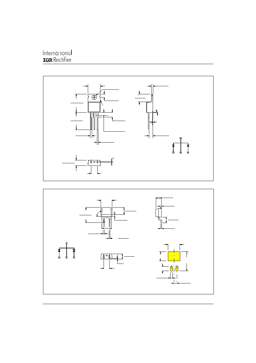
Outline Table
3.78 (0.15)
3.54 (0.14)
10.54 (0.41)
MAX.
DIA.
15.24 (0.60)
14.84 (0.58)
2.92 (0.11)
2.54 (0.10)
1
TERM 2
14.09 (0.55)
13.47 (0.53)
3.96 (0.16)
3.55 (0.14)
0.94 (0.04)
0.69 (0.03)
4.57 (0.18)
4.32 (0.17)
3
0.61 (0.02) MAX.
5.08 (0.20) REF.
1.32 (0.05)
1.22 (0.05)
6.48 (0.25)
6.23 (0.24)
2∞
0.10 (0.004)
1.40 (0.05)
1.15 (0.04)
2.89 (0.11)
2.64 (0.10)
1
3
2.04 (0.080) MAX.
2
2
Dimensions in millimeters and (inches)
Conform to JEDEC outline TO-220AB
2
BASE
COMMON
CATHODE
1
2
3
ANODE
COMMON
CATHODE
ANODE
1
2
10.16 (0.40)
REF.
8.89 (0.35)
4.57 (0.18)
4.32 (0.17)
0.61 (0.02) MAX.
5.08 (0.20) REF.
1.32 (0.05)
1.22 (0.05)
1
3
6.47 (0.25)
6.18 (0.24)
93∞
REF.
2.61 (0.10)
2.32 (0.09)
5.28 (0.21)
4.78 (0.19)
4.69 (0.18)
4.20 (0.16)
0.55 (0.02)
0.46 (0.02)
14.73 (0.58)
15.49 (0.61)
1.40 (0.055)
1.14 (0.045)
3X
0.93 (0.37)
0.69 (0.27)
2X
11.43 (0.45)
17.78 (0.70)
8.89 (0.35)
3.81 (0.15)
2.08 (0.08)
2X
2.54 (0.10)
2X
MINIMUM RECOMMENDED FOOTPRINT
2
Dimensions in millimeters and (inches)
Conform to JEDEC outline D
2
Pak (SMD-220)
2
BASE
COMMON
CATHODE
1
2
3
ANODE
COMMON
CATHODE
ANODE
1
2