 | –≠–ª–µ–∫—Ç—Ä–æ–Ω–Ω—ã–π –∫–æ–º–ø–æ–Ω–µ–Ω—Ç: 95SQ015 | –°–∫–∞—á–∞—Ç—å:  PDF PDF  ZIP ZIP |

SCHOTTKY RECTIFIER
9 Amp
95SQ015
Bulletin PD-2.273 rev. C 05/02
1
www.irf.com
Dimensions in millimeters and inches
Conforms to JEDEC Outline DO - 204AR
CASE STYLE AND DIMENSIONS
Major Ratings and Characteristics
I
F(AV)
Rectangular
9
A
waveform
V
RRM
15
V
I
FSM
@ tp = 5 µs sine
2900
A
V
F
@
9 Apk, T
J
= 75∞C
0.25
V
T
J
range
- 55 to 100
∞C
Characteristics
95SQ015 Units
Description/Features
The 95SQ015 axial leaded Schottky rectifier has been opti-
mized for ultra low forward voltage drop specifically for the
OR-ing of parallel power supplies. The proprietary barrier
technology allows for reliable operation up to 100∞ C junction
temperature. Typical applications are in parallel switching
power supplies, converters, reverse battery protection, and
redundant power subsystems.
125∞C T
J
operation (V
R
< 5V)
Optimized for OR-ing applications
Ultra low forward voltage drop
High frequency operation
Guard ring for enhanced ruggedness and long term
reliability
High purity, high temperature epoxy encapsulation for
enhanced mechanical strength and moisture resistance

95SQ015
Bulletin PD-2.273 rev. C 05/02
2
www.irf.com
Part number
95SQ015
V
R
Max. DC Reverse Voltage (V)
15
V
RWM
Max. Working Peak Reverse Voltage (V)
25
Voltage Ratings
I
F(AV)
Max. Average Forward Current
9
A
50% duty cycle @ T
C
= 55∞ C, rectangular wave form
* See Fig. 5
I
FSM
Max. Peak One Cycle Non-Repetitive
2900
5µs Sine or 3µs Rect. pulse
Surge Current * See Fig. 7
400
10ms Sine or 6ms Rect. pulse
E
AS
Non-Repetitive Avalanche Energy
4.50
mJ
T
J
= 25 ∞C, I
AS
= 1 Amps, L = 9 mH
I
AR
Repetitive Avalanche Current
1
A
Current decaying linearly to zero in 1 µsec
Frequency limited by T
J
max. V
A
= 3 x V
R
typical
Parameters
95SQ Units
Conditions
Absolute Maximum Ratings
A
Following any rated
load condition and
with rated V
RRM
applied
V
FM
Max. Forward Voltage Drop (1)
0.31
V
@ 9A
* See Fig. 1
0.37
V
@ 18A
0.25
V
@ 9A
0.31
V
@ 18A
I
RM
Max. Reverse Leakage Current (1)
7
mA
T
J
= 25 ∞C
* See Fig. 2
348
mA
T
J
= 100 ∞C
310
mA
T
J
= 100 ∞C
V
R
= 12V
190
mA
T
J
= 100 ∞C
V
R
= 5V
C
T
Max. Junction Capacitance
1300
pF
V
R
= 5V
DC
, (test signal range 100Khz to 1Mhz) 25 ∞C
L
S
Typical Series Inductance
10.0
nH
Measured lead to lead 5mm from body
dv/dt Max. Voltage Rate of Change
10000
V/ µs
(Rated V
R
)
T
J
= 25 ∞C
T
J
= 75 ∞C
V
R
= rated V
R
Parameters
95SQ Units
Conditions
Electrical Specifications
(1) Pulse Width < 300µs, Duty Cycle < 2%
T
J
Max. Junction Temperature Range
-55 to 125
∞C
T
stg
Max. Storage Temperature Range
-55 to 150
∞C
R
thJL
Max. Thermal Resistance Junction
8.0
∞C/W DC operation * See Fig. 4
to Lead
1/8 inch lead leangth
R
thJA
Typical Thermal Resistance,
44
∞C/W
Junction to Air
wt
Approximate Weight
1.4(0.049) g (oz.)
Case Style
DO - 204AR
JEDEC
Thermal-Mechanical Specifications
Parameters
95SQ Units
Conditions

95SQ015
Bulletin PD-2.273 rev. C 05/02
3
www.irf.com
Fig. 2 - Typical Values of Reverse Current
Vs. Reverse Voltage
Fig. 3 - Typical Junction Capacitance
Vs. Reverse Voltage
Fig. 4 - Maximum Thermal Impedance Z
thJL
Characteristics
Fig. 1 - Maximum Forward Voltage Drop Characteristics
.1
1
10
100
0
.1
.2
.3
.4
.5
.6
.7
.8
FM
F
In
s
t
a
n
ta
n
e
o
u
s
F
o
r
w
a
r
d
C
u
r
r
e
n
t
-
I (
A
)
Forward Voltage Drop - V (V)
T = 100∞C
T = 75∞C
T = 25∞C
J
J
J
.1
1
10
100
1000
0
5
10
15
R
R
75∞C
50∞C
25∞C
Reverse Voltage - V (V)
R
ev
e
r
s
e
C
u
r
r
e
n
t
-
I (
m
A)
T = 100∞C
J
100
1000
10000
0
5
10
15
20
25
30
T = 25∞C
J
Reverse Voltage - V (V)
R
T
J
u
n
c
ti
o
n
C
a
p
a
c
i
ta
n
c
e
-
C
(
p
F
)
.01
.1
1
10
.00001
.0001
.001
.01
.1
1
10
100
D = 0.33
D = 0.50
D = 0.25
D = 0.17
D = 0.08
1
t , Rectangular Pulse Duration (Seconds)
Th
e
r
m
a
l
Im
p
e
d
a
n
c
e
-
Z
(
∞
C
/
W
)
Single Pulse
(Thermal Resistance)
th
J
L
2
t
1
t
P
DM
Notes:
1. Duty factor D = t / t
2. Peak T = P x Z + T
1
J
DM
C
2
thJL
= 1/8 inch
95SQ015
Bulletin PD-2.273 rev. C 05/02
4
www.irf.com
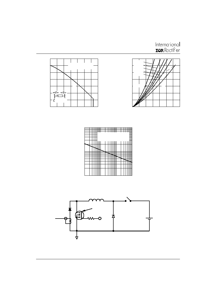
Fig. 8 - Unclamped Inductive Test Circuit
Fig. 5 - Maximum Allowable Case Temperature
Vs. Average Forward Current
Fig. 6 - Forward Power Loss Characteristics
Fig. 7 - Maximum Non-Repetitive Surge Current
0
.5
1
1.5
2
2.5
3
3.5
0
2
4
6
8
10
12
14
DC
A
v
e
r
a
g
e
P
o
w
e
r L
o
s
s
- (W
a
tts
)
F(AV)
D = 0.08
D = 0.17
D = 0.25
D = 0.33
D = 0.50
RMS Limit
Average Forward Current - I (A)
70
75
80
85
90
95
100
105
0
2
4
6
8
10
12
14
DC
A
llo
w
ab
l
e
C
as
e T
e
m
p
e
ra
t
u
re
-
(∞
C
)
Average Forward Current - I (A)
F(AV)
95SQ015
R (DC) = 8.0∞C/W
thJL
= 1/8 inch
100
1000
10000
10
100
1000
10000
FS
M
p
Non-Rep
e
ti
ti
ve Surge Cur
r
en
t - I (A)
At Any Rated Load Condition
And With Rated V Applied
Following Surge
RRM
Square Wave Pulse Duration - t (microsec)
FR EE-W H E EL
D IO D E
40H FL40 S02
C UR RE N T
M O N ITO R
H IG H-SPE ED
SW ITC H
IRFP460
L
D UT
R g = 25 ohm
V d = 25 V olt
+
95SQ015
Bulletin PD-2.273 rev. C 05/02
5
www.irf.com
IR WORLD HEADQUARTERS: 233 Kansas St., El Segundo, California 90245, USA Tel: (310) 252-7105
TAC Fax: (310) 252-7309
Visit us at www.irf.com for sales contact information. 05/02
Data and specifications subject to change without notice.
This product has been designed and qualified for Industrial Level.
Qualification Standards can be found on IR's Web site.
Ordering Information Table
Device Code
1
2
4
3
1
-
95 = current x 10
2
-
S = DO-204AR
3
-
Q = Schottky Q Series
4
-
Voltage Rating (15V)
5
-
TR = Tape & Reel package (1500 pcs)
-
= Box package (200 pcs)
95
S
Q
015
TR
5