09/11/02
www.irf.com
1
ADVANCED ANALOG
HIGH RELIABILITY
HYBRID DC/DC CONVERTERS
ASA28XXS SERIES
Description
n
Up To 5 Watt Output Power
n
5, 12,15 Volt Outputs
n
High Reliability
n
Wide Input Voltage Range -16 To 40 Volts
n
Indefinite Short Circuit and Overload
Protection
n
Popular Industry Standard Pin-Out
n
Military Screening Available
n
Parallel Seam Welded Package
n
No External Capacitors Required
n
Input Voltage Surge Protected to
MIL-STD-704A
n
Under Voltage Lockout
n
Available as Standard Military Drawing
Features
ASA
28V Input, Single Output
The ASA28XXS Series of DC/DC converters are high
reliability thick film hybrid converters that use flyback
topology operating at a nominal frequency of 550Khz.
High input to output isolation is achieved through the
use of transformers in the flyback power and feedback
circuits.
The advanced feedback design provides fast loop re-
sponse for superior line and load transient characteris-
tics and offers greater reliability than devices incorpo-
rating optical feedback circuits.
This device is designed to meet MIL-STD-704D input
requirements offering full performance over a 16 to 40
volt input range. Output Power of up to 5 watts is avail-
able.
Connecting the inhibit pin (pin 5) to the input common
(pin 7) will cause the converter to shut down. It is rec-
ommended that the inhibit pin be driven by an open
collector device capable of sinking at least 400
µ
A. The
open circuit voltage of the inhibit pin is 11.5 ±0.5 volts.
These converters are manufactured in a facility fully
qualified to MIL-PRF-38534. All processes used to
manufacture these converters have been qualified
thereby enabling Advanced Analog to deliver fully com-
pliant devices. Three standard temperature grades are
offered with the screening options. Refer to Screening
Level section. The CH grade converters are fully com-
pliant to MIL-PRF-38534 for class H. The HB grade
converters are processed with the same screening as
the CH grade, but do not have class H element evalua-
tion as required by MIL-PRF-38534. These two grades
are fully tested and operate over the full military tem-
perature range without derating of output power. A
commercial grade is also available. Variations in elec-
trical, mechanical and screening requirements can be
accommodated. Extensive computer simulation using
complex modeling allows design modifications
to be examined. Contact Advanced Analog with
specific requirements.
PD - 94539
2
www.irf.com
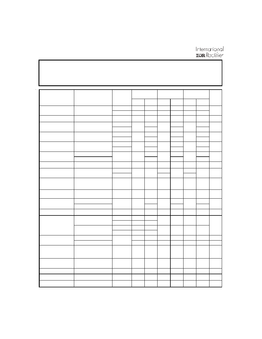
ASA28XXS Series
Specifications
For Notes to Specifications, refer to page 3
ABSOLUTE MAXIMUM RATINGS
Input Voltage
-0.5 V to 50 V Continuous. 80 V, 100 mSec
Power Output
Internally limited (6.5 W typical)
Soldering
300∞C for 10 Sec.
Temperature Range
Operating
-55∞C to +125∞C Case
Storage
-65∞C to +150∞C
ASA2805S/xx
ASA2812S/xx
ASA2815S/xx
TEST
Conditions
-55∞
T
C
+125∞C
V
IN
= 28V dc ±5% C
L
= 0
unless otherwise specified
Group A
Subgroups
Min Max Min Max Min Max Unit
1
4.95 5.05 11.88 12.12 14.85 15.15
Output voltage
I
OUT
= 0
2,
3
4.90 5.10 11.76 12.24 14.70 15.30
V
Output current
1
V
IN
= 16, 28, and 40 V dc
1, 2, 3
1000
417
333
mA
1 190
200
200
Output ripple voltage
2
V
IN
= 16, 28 and 40 V dc
2, 3
475
290
290
mV
PP
1 25
±25
±25
Line regulation
V
IN
= 16, 28, and 40 V dc
I
OUT
= 0, 50%, 100% I
MAX
2, 3
50
±50
±50
mV
1 25
±25
±25
Load regulation
V
IN
= 16, 28, and 40 V dc
I
OUT
= 0, 50%, 100% I
MAX
2, 3
50
±50
±50
mV
I
OUT
= 0 Pin 5 to Pin 7
18
18
18
Input current
I
OUT
= 0 Pin5 open
1, 2, 3
50
50
50
mA
Input ripple current
2
I
OUT
= I
MAX
1, 2, 3
100
100
100
mA
PP
1 71
71
Efficiency
I
OUT
= I
MAX
2, 3
66
68
68
%
Isolation - Input to
output or any pin to
case
V
TEST
500 Vdc, Tc= +25∞C
1 100 100 100 M
Capacitive load
3, 4
No effect on dc
performance, Tc = +25∞C
4
500 200 200
µ
f
Overload
5
4.0 4.0 4.0
Power dissipation, load
fault
Short circuit
1, 2, 3
2.0
2.0
2.0
W
Switching frequency
4
I
OUT
= I
MAX
4,
5,
6 500 600 500 600 500 600 KHz
4 -300
+300
Ω I
MAX
Û
I
MAX
5, 6
-450
+450
-450 +450 -400 +450
4 -500
+500
Output response to step
transient load changes
6
0 mA
Û
I
MAX
5, 6
-750
+700
-750 +750 -800 +750
mV pk
I
OUT
= I
MAX
200 100 100
µ
S
Recovery time, step
transient load changes
0 mA
Û
Ω I
MAX
4, 5, 6
1 1 1
ms
Output response
transient step line
changes
4 8
Input step 16
Û
40 V dc
I
OUT
= I
MAX
4,
5,
6 500 1000 1000
mV
pk
Recovery time transient
step line changes
4, 7, 8
Input step 16
Û
40 V dc
I
OUT
= I
MAX
4, 5, 6
800
800
800
µ
S
Turn on overshoot
I
OUT
= 0 mA, I
MAX
4, 5, 6
600
600
600
mV pk
Turn on delay
9
I
OUT
= 0 or I
MAX
4,
5,
6 20 25 25
ms
Load fault recovery
4
4,
5,
6 20 25 25
ms
www.irf.com
3
ASA28XXS Series
Notes to Specifications
1.
Parameter guaranteed and measured during line and load regulation tests.
2.
Bandwidth guaranteed by design. Tested for 20 kHz to 2 MHz.
3.
Capacitive load may be any value from 0 to the maximum limit without compromising dc performance. A capacitive load in excess
of the maximum limit will not disturb loop stability but may interfere with the operation of the load fault detection circuitry,
appearing as a short circuit during turn-on.
4.
Parameter shall be tested as part of design characterization and after design or process changes.
5.
An overload is that condition of load in excess of rated load but less than that necessary to trigger the short circuit protection
and is the condition of maximum power dissipation.
6.
Load step transition time between 2 and 10 microseconds.
7.
Recovery time is measured from the initiation of the transient to where V
OUT
has returned to within ±1 percent of V
OUT
at 50
percent load.
8.
Input step transition time between 2 and 10 microseconds.
9.
Turn-on delay time measurement is for either a step application of power at the input or the removal of a ground signal from the
inhibit pin (pin 2) while power is applied to the input.
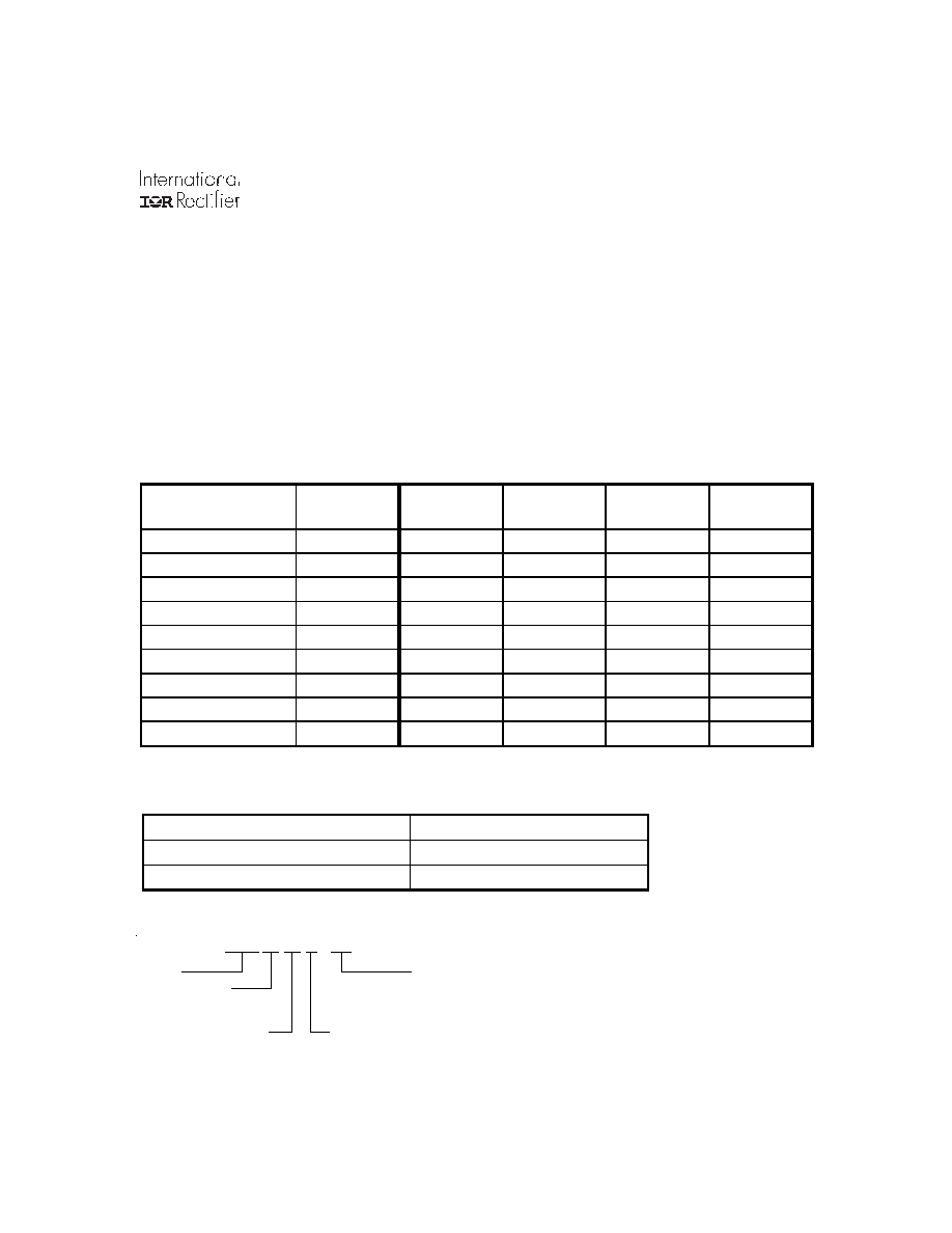
Available Screening Levels and Process Variations for ASA28XXS Series
Requirement
MIL-STD-883
Method
No
Suffix
ES
Suffix
HB
Suffix
CH
Suffix
Temperature Range
-20∞C to +85∞C
-55∞C to +125∞C
-55∞C to +125∞C
-55∞C to +125∞C
Element
Evaluation
MIL-PRF-38534
Internal Visual
2017
¨
¸
¸
¸
Temperature Cycle
1010
Cond B
Cond C
Cond C
Constant Acceleration
2001,
500g
Cond A
Cond A
Burn-in 1015
48hrs
@
85
∞
C
48hrs @ 125∞C
160hrs @ 125∞C
160hrs @ 125∞C
Final Electrical (Group A)
MIL-PRF-38534
25∞C
25∞C
-55, +25, +125∞C
-55, +25, +125∞C
Seal, Fine & Gross
1014
Cond C
Cond A, C
Cond A, C
Cond A, C
External Visual
2009
¨
¸
¸
¸
*
per Commercial Standards
Available Standard Military Drawing (SMD) Cross Reference
ASA 28 05 S / CH
M o d e l
Input Voltage
28 = 28V
Output Voltage
5 = ±5, 12 = ±12,
15 = ±15
O u t p u t s
S = Single
D = Dual
Screening
≠
, ES, HB, CH
Part Numbering
ASA2805S/CH 5962-9462901
ASA2812S/CH 5962-9463101
ASA2815S/CH 5962-9463001
4
www.irf.com
ASA28XXS Series
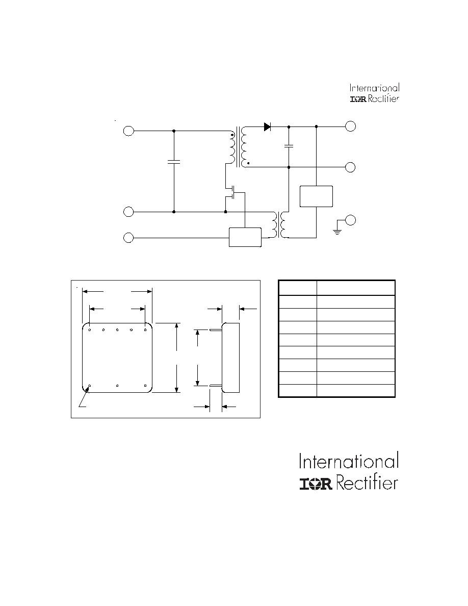
ASA28XXS Pin Designation
WORLD HEADQUARTERS: 233 Kansas St., El Segundo, California 90245, Tel: (310) 322 3331
ADVANCED ANALOG: 2270 Martin Av., Santa Clara, California 95050, Tel: (408) 727-0500
Visit us at www.irf.com for sales contact information.
Data and specifications subject to change without notice. 09/02
ASA28XXS Block Diagram
Controller
Error
Amplifier
1
2
8
6
7
5
C a s e
R e t u r n
+ O u t p u t
E n a b l e
R e t u r n
+Input
0.800
±.005
1.075
0.220
0.270
1.075
0.800
0.025 ± .003 Dia Pins
1
2
3
4
5
6
8
7
ASA28XXS Case Outline
Pin No.
Designation
1 Positive
Output
2 Output
Return
3 N/C
4 N/C
5 Enable
6 Positive
Input
7 Input
Return
8 Case