 | ÐлекÑÑоннÑй компоненÑ: CPV362M4F | СкаÑаÑÑ:  PDF PDF  ZIP ZIP |
Äîêóìåíòàöèÿ è îïèñàíèÿ www.docs.chipfind.ru
CPV362M4F
PD -5.046
Fast IGBT
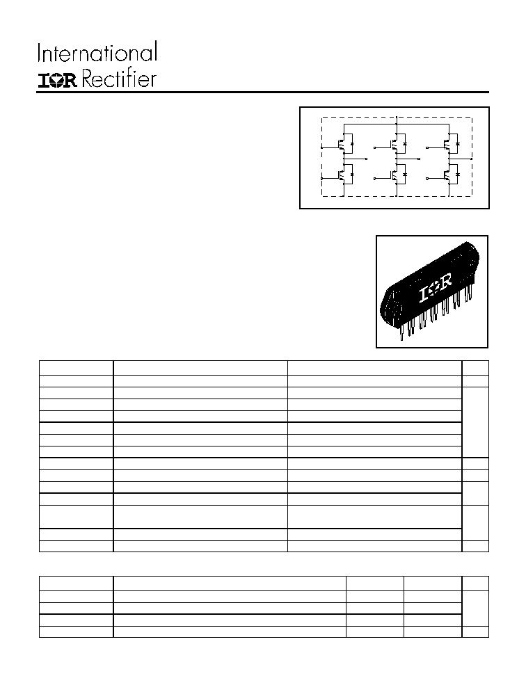
IGBT SIP MODULE
Features
Description
3
6
7
1 3
1 9
1 8
1 5
1 0
1 6
4
9
1 2
D 1
D 3
D 5
D 2
D 4
D 6
Q 1
Q 2
Q 3
Q 4
Q 5
Q 6
1
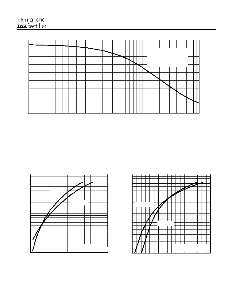
Output Current in a Typical 5.0 kHz Motor Drive
Product Summary
· Fully isolated printed circuit board mount package
· Switching-loss rating includes all "tail" losses
· HEXFRED
TM
soft ultrafast diodes
· Optimized for medium operating (1 to 10 kHz)
See Fig. 1 for Current vs. Frequency curve
11 A
RMS
per phase (3.1 kW total) with T
C
= 90°C, T
J
= 125°C, Supply Voltage 360Vdc,
Power Factor 0.8, Modulation Depth 115% (See Figure 1)
The IGBT technology is the key to International Rectifier's advanced line of
IMS (Insulated Metal Substrate) Power Modules. These modules are more
efficient than comparable bipolar transistor modules, while at the same time
having the simpler gate-drive requirements of the familiar power MOSFET.
This superior technology has now been coupled to a state of the art materials
system that maximizes power throughput with low thermal resistance. This
package is highly suited to motor drive applications and where space is at a
premium.
9/16/97
IMS-2
Parameter
Typ.
Max.
Units
R
JC
(IGBT)
Junction-to-Case, each IGBT, one IGBT in conduction
5.5
R
JC
(DIODE)
Junction-to-Case, each diode, one diode in conduction
9.0
°C/W
R
CS
(MODULE)
Case-to-Sink, flat, greased surface
0.1
Wt
Weight of module
20 (0.7)
g (oz)
Absolute Maximum Ratings
Thermal Resistance
Parameter
Max.
Units
V
CES
Collector-to-Emitter Voltage
600
V
I
C
@ T
C
= 25°C
Continuous Collector Current, each IGBT
8.8
I
C
@ T
C
= 100°C
Continuous Collector Current, each IGBT
4.8
I
CM
Pulsed Collector Current
26
A
I
LM
Clamped Inductive Load Current
26
I
F
@ T
C
= 100°C
Diode Continuous Forward Current
3.4
I
FM
Diode Maximum Forward Current
26
V
GE
Gate-to-Emitter Voltage
±20
V
V
ISOL
Isolation Voltage, any terminal to case, 1 minute
2500
V
RMS
P
D
@ T
C
= 25°C
Maximum Power Dissipation, each IGBT
23
W
P
D
@ T
C
= 100°C
Maximum Power Dissipation, each IGBT
9.1
T
J
Operating Junction and
-40 to +150
T
STG
Storage Temperature Range
°C
Soldering Temperature, for 10 sec.
300 (0.063 in. (1.6mm) from case)
Mounting torque, 6-32 or M3 screw
5-7 lbf·in (0.55-0.8 N·m)
CPV362M4F
Parameter
Min. Typ. Max. Units
Conditions
Q
g
Total Gate Charge (turn-on)
30
45
I
C
= 4.8A
Q
ge
Gate - Emitter Charge (turn-on)
4.0
6.0
nC
V
CC
= 400V
Q
gc
Gate - Collector Charge (turn-on)
13
20
See Fig. 8
t
d(on)
Turn-On Delay Time
49
T
J
= 25°C
t
r
Rise Time
22
ns
I
C
= 4.8A, V
CC
= 480V
t
d(off)
Turn-Off Delay Time
200
300
V
GE
= 15V, R
G
= 50
t
f
Fall Time
214
320
Energy losses include "tail" and
E
on
Turn-On Switching Loss
0.23
diode reverse recovery
E
off
Turn-Off Switching Loss
0.33
mJ
See Fig. 9, 10, 18
E
ts
Total Switching Loss
0.45 0.70
t
d(on)
Turn-On Delay Time
48
T
J
= 150°C, See Fig. 10,11, 18
t
r
Rise Time
25
ns
I
C
= 4.8A, V
CC
= 480V
t
d(off)
Turn-Off Delay Time
435
V
GE
= 15V, R
G
= 50
t
f
Fall Time
364
Energy losses include "tail" and
E
ts
Total Switching Loss
0.93
mJ
diode reverse recovery
C
ies
Input Capacitance
340
V
GE
= 0V
C
oes
Output Capacitance
63
pF
V
CC
= 30V
See Fig. 7
C
res
Reverse Transfer Capacitance
5.9
= 1.0MHz
t
rr
Diode Reverse Recovery Time
37
55
ns
T
J
= 25°C See Fig.
55
90
T
J
= 125°C 14 I
F
= 8.0A
I
rr
Diode Peak Reverse Recovery Current
3.5
50
A
T
J
= 25°C See Fig.
4.5
8.0
T
J
= 125°C 15 V
R
= 200V
Q
rr
Diode Reverse Recovery Charge
65
138
nC
T
J
= 25°C See Fig.
124
360
T
J
= 125°C 16 di/dt = 200A/µs
di
(rec)M
/dt
Diode Peak Rate of Fall of Recovery
240
A/µs
T
J
= 25°C See Fig.
During t
b
210
T
J
= 125°C 17
Pulse width
80µs; duty factor
0.1%.
V
CC
=80%(V
CES
), V
GE
=20V, L=10µH,
R
G
= 50
, ( See fig. 19 )
Pulse width 5.0µs, single
shot.
Repetitive rating; V
GE
=20V, pulse width
limited by max. junction temperature.
( See fig. 20 )
Notes:
Switching Characteristics @ T
J
= 25°C (unless otherwise specified)
Electrical Characteristics @ T
J
= 25°C (unless otherwise specified)
Parameter
Min. Typ. Max. Units
Conditions
V
(BR)CES
Collector-to-Emitter Breakdown Voltage
600
V
V
GE
= 0V, I
C
= 250µA
V
(BR)CES
/
T
J
Temperature Coeff. of Breakdown Voltage
0.72
V/°C
V
GE
= 0V, I
C
= 1.0mA
V
CE(on)
Collector-to-Emitter Saturation Voltage
1.41
1.7
I
C
= 4.8A
V
GE
= 15V
1.66
V
I
C
= 8.8A
See Fig. 2, 5
1.42
I
C
= 4.8A, T
J
= 150°C
V
GE(th)
Gate Threshold Voltage
3.0
6.0
V
CE
= V
GE
, I
C
= 250µA
V
GE(th)
/
T
J
Temperature Coeff. of Threshold Voltage
-11
mV/°C
V
CE
= V
GE
, I
C
= 250µA
g
fe
Forward Transconductance
2.9
5.0
S
V
CE
= 100V, I
C
= 4.8A
I
CES
Zero Gate Voltage Collector Current
250
µA
V
GE
= 0V, V
CE
= 600V
1700
V
GE
= 0V, V
CE
= 600V, T
J
= 150°C
V
FM
Diode Forward Voltage Drop
1.4
1.7
V
I
C
= 8.0A
See Fig. 13
1.3
1.6
I
C
= 8.0A, T
J
= 150°C
I
GES
Gate-to-Emitter Leakage Current
±100
nA
V
GE
= ±20V
CPV362M4F
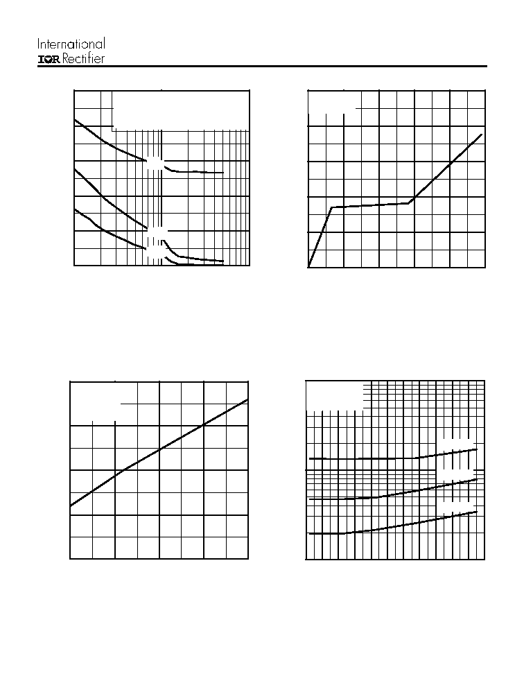
Fig. 1 - Typical Load Current vs. Frequency
(Load Current = I
RMS
of fundamental)
Fig. 2 - Typical Output Characteristics
Fig. 3 - Typical Transfer Characteristics
1
10
100
1
10
V , Collector-to-Emitter Voltage (V)
I , Collector-to-Emitter Current (A)
CE
C
V = 15V
20µs PULSE WIDTH
GE
T = 25 C
J
o
T = 150 C
J
o
1
10
100
5
6
7
8
9
10
11
12
13
14
V , Gate-to-Emitter Voltage (V)
I , Collector-to-Emitter Current (A)
GE
C
V = 50V
5µs PULSE WIDTH
CC
T = 25 C
J
o
T = 150 C
J
o
0.1
1
10
100
0
1
2
3
4
5
6
7
8
9
f, Frequency (KHz)
LOAD CURRENT (A)
T c = 9 0° C
T j = 1 25 ° C
P ow er F ac tor = 0 .8
M o d ula tio n D ep th = 1 .15
V c c = 50 % o f R a ted V o lta g e
0.00
0.29
0.58
0.88
Total Output Power (kW)
1.75
2.05
1.17
1.46
2.34
2.63
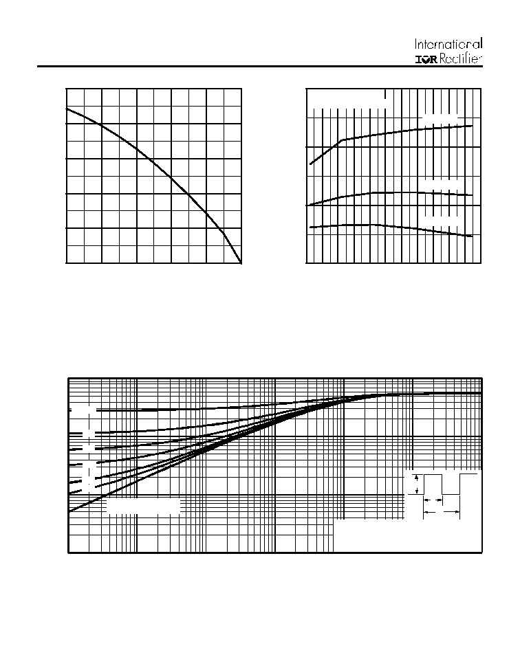
CPV362M4F
Fig. 6 - Maximum Effective Transient Thermal Impedance, Junction-to-Case
Fig. 5 - Typical Collector-to-Emitter Voltage
vs. Junction Temperature
Fig. 4 - Maximum Collector Current vs. Case
Temperature
0.01
0 .1
1
10
0.000 01
0.00 01
0 .00 1
0.01
0.1
1
10
t , R e ct an g ula r P u ls e D ur a t io n (s e c)
1
th
J
C
D = 0.50
0.01
0.02
0.05
0.10
0.20
SINGLE PULSE
(T H ERMA L RES PO NSE)
T
h
er
m
a
l
R
e
s
p
ons
e (
Z
)
P
t
2
1
t
D M
N otes :
1. D u ty fact or D = t / t
2. P e ak T = P x Z + T
1
2
J
D M
th JC
C
-60 -40 -20
0
20
40
60
80 100 120 140 160
1.0
1.5
2.0
2.5
T , Junction Temperature ( C)
V , Collector-to-Emitter Voltage(V)
J
°
CE
V = 15V
80 us PULSE WIDTH
GE
I = A
9.6
C
I = A
4.8
C
I = A
2.4
C
C)
25
50
75
100
125
150
0
2
4
6
8
10
T , Case Temperature ( C)
Maximum DC Collector Current(A)
C
°
CPV362M4F
Fig. 7 - Typical Capacitance vs.
Collector-to-Emitter Voltage
Fig. 8 - Typical Gate Charge vs.
Gate-to-Emitter Voltage
Fig. 9 - Typical Switching Losses vs. Gate
Resistance
Fig. 10 - Typical Switching Losses vs.
Junction Temperature
1
10
100
0
200
400
600
800
1000
V , Collector-to-Emitter Voltage (V)
C, Capacitance (pF)
CE
V
C
C
C
=
=
=
=
0V,
C
C
C
f = 1MHz
+ C
+ C
C SHORTED
GE
ies
ge
gc ,
ce
res
gc
oes
ce
gc
Cies
Coes
Cres
-60 -40 -20
0
20
40
60
80
100 120 140 160
0.1
1
10
T , Junction Temperature ( C )
Total Switching Losses (mJ)
J
°
R = 50Ohm
V = 15V
V = 480V
G
GE
CC
I = A
9.6
C
I = A
4.8
C
I = A
2.4
C
50
0
6
12
18
24
30
0
4
8
12
16
20
Q , Total Gate Charge (nC)
V , Gate-to-Emitter Voltage (V)
G
GE
V
= 400V
I
= 4.8A
CC
C
10
20
30
40
50
0.42
0.43
0.44
0.45
0.46
R , Gate Resistance (Ohm)
Total Switching Losses (mJ)
G
V = 480V
V = 15V
T = 25 C
I = 4.8A
CC
GE
J
C
°
()