 | ÐлекÑÑоннÑй компоненÑ: HFB25HJ20 | СкаÑаÑÑ:  PDF PDF  ZIP ZIP |
Äîêóìåíòàöèÿ è îïèñàíèÿ www.docs.chipfind.ru
7/9/01
· Reduced RFI and EMI
· Reduced Snubbing
· Extensive Characterization of Recovery Parameters
· Hermetic
· Surface Mount
Features
Description
Ultrafast, Soft Recovery Diode
FRED
V
R
= 200V
I
F(AV)
= 25A
t
rr
= 35ns
Note:
Q
D.C. = 50% rect. wave
R
1/2 sine wave, 60 Hz , P.W. = 8.33 ms
HFB25HJ20
www.irf.com
1
Parameter
Max.
Units
V
R
Cathode to Anode Voltage
200
V
I
F(AV)
Continuous Forward Current,
Q
T
C
= 106°C
25
I
FSM
Single Pulse Forward Current,
R
T
C
= 25°C
150
P
D
@ T
C
= 25°C
Maximum Power Dissipation
70
W
T
J,
T
STG
Operating Junction and Storage Temperature Range
-55 to +150
°C
A
Absolute Maximum Ratings
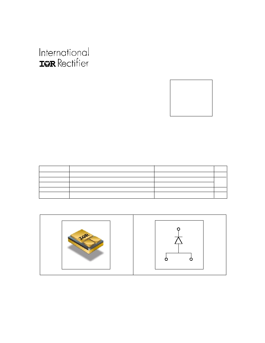
ANODE
ANODE
CATHODE
CASE STYLE
SMD-0.5
PD-94150B
These Ultrafast, soft recovery diodes are optimized to reduce losses and EMI/RFI in high frequency power
conditioning systems. An extensive characterization of the recovery behavior for different values of current,
temperature and di/dt simplifies the calculations of losses in the operating conditions. The softness of the recovery
eliminates the need for a snubber in most applications. These devices are ideally suited for power converters, motors
drives and other applications where switching losses are significant portion of the total losses.

2
www.irf.com
HFB25HJ20
See Fig. 2
Parameter
Min. Typ. Max. Units
Test Conditions
V
BR
Cathode Anode Breakdown Voltage 200
--
--
V
I
R
= 100µA
V
F
Forward Voltage
--
--
1.18
I
F
= 25A, T
J
=-55°C
Electrical Characteristics @ T
J
= 25°C (unless otherwise specified)
L
S
Series Inductance
--
4.8
--
nH
Measured from center of cathod
pad to center of anode pad
C
T
Junction Capacitance, See Fig. 3
--
--
78
pF
V
R
= 200V
I
R
Reverse Leakage Current
--
--
10
µA
V
R
= V
R
Rated
See Fig. 2
--
--
250
µA
V
R
= V
R
Rated, T
J
= 125°C
A/µs
nC
A
Dynamic Recovery Characteristics @ T
J
= 25°C (unless otherwise specified)
A/µs
nC
A
Parameter Min. Typ. Max. Units Test Conditions
t
rr
Reverse Recovery Time
--
--
35
ns
I
F
= 1.0A,V
R
= 30V, di
f
/dt = 200A/µs
t
rr1
Reverse Recovery Time
--
28
--
ns
T
J
= 25°C See Fig.
t
rr2
--
43
--
T
J
= 125°C 5
I
F
= 25A
I
RRM1
Peak Recovery Current
--
3.9
--
T
J
= 25°C See Fig.
I
RRM2
--
6.1
--
T
J
= 125°C 6
V
R
= 160V
Q
rr1
Reverse Recovery Charge
--
61
--
T
J
= 25°C See Fig.
Q
rr2
--
146 --
T
J
= 125°C 7
di
f
/dt = 200A/µs
di
(rec)M
/dt1
Peak Rate of Fall of Recovery Current
--
820
--
T
J
= 25°C See Fig.
di
(rec)M
/dt2
During t
b
--
1560 --
T
J
= 125°C 8
Thermal - Mechanical Characteristics
Parameter
Typ.
Max.
Units
R
thJC
Junction-to-Case
--
1.76
Wt
Weight
1.0
--
g
°C/W
See Fig. 1
--
-- 0.94
I
F
= 10A, T
J
= 25°C
--
-- 1.07
I
F
= 25A, T
J
= 25°C
-- -- 1.19
I
F
= 50A, T
J
= 25°C
-- -- 0.88
I
F
= 25A, T
J
=125°C
V
www.irf.com
3
HFB25HJ20
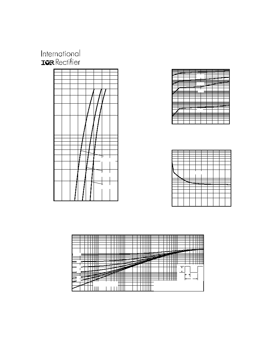
Fig. 4 - Maximum Thermal Impedance Z
thjc
Characteristics
Fig. 2 - Typical Reverse Current Vs. Reverse
Voltage
Fig. 3 - Typical Junction Capacitance Vs.
Reverse Voltage
Fig. 1 - Maximum Forward Voltage Drop Vs.
Instantaneous Forward Current
0.0
0.2
0.4
0.6
0.8
1.0
1.2
1.4
1.6
Forward Voltage Drop - V F (V)
1
10
100
Instantaneous Forward Current - I
F
(A)
Tj = -55°C
Tj = 125°C
Tj = 25°C
0
40
80
120
160
200
Reverse Voltage - V R (V)
0.0001
0.001
0.01
0.1
1
10
Reverse Current - I
R
(µA)
125°C
75°C
25°C
100°C
0.01
0.1
1
10
0.00001
0.0001
0.001
0.01
0.1
1
Notes:
1. Duty factor D = t / t
2. Peak T = P
x Z
+ T
1
2
J
DM
thJC
C
P
t
t
DM
1
2
t , Rectangular Pulse Duration (sec)
Thermal Response
(Z )
1
thJC
0.01
0.02
0.05
0.10
0.20
D = 0.50
SINGLE PULSE
(THERMAL RESPONSE)
0
40
80
120
160
200
Reverse Voltage - VR (V)
10
100
1000
Junction Capacitance - C
T
(pF)
TJ = 25°C
4
www.irf.com
HFB25HJ20
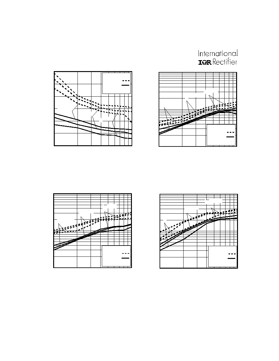
Fig. 7 - Typical Stored Charge Vs. di
f
/dt
Fig. 8 - Typical di
(rec)M
/dt Vs. di
f
/dt
Fig. 5 - Typical Reverse Recovery Vs. di
f
/dt,
Fig. 6 - Typical Recovery Current Vs. di
f
/dt,
100
1000
dif / dt - ( A / µs )
20
30
40
50
t rr
- ( ns )
VR = 160V
TJ = 125°C
TJ = 25°C
IF = 12.5A
IF = 50A
IF = 25A
100
1000
dif / dt - ( A / µs )
1
10
100
I RRM
- ( A )
VR = 160V
TJ = 125°C
TJ = 25°C
IF = 12.5A
IF = 50A
IF = 25A
100
1000
dif / dt - ( A / µs )
10
100
1000
Q
rr
- ( nC )
VR = 160V
TJ = 125°C
TJ = 25°C
IF = 12.5A
IF = 50A
IF = 25A
100
1000
dif / dt - ( A / µs )
100
1000
10000
di
( rec )M
/ dt - ( A / µs )
VR = 160V
TJ = 125°C
TJ = 25°C
IF = 12.5A
IF = 50A
IF = 25A
www.irf.com
5
HFB25HJ20
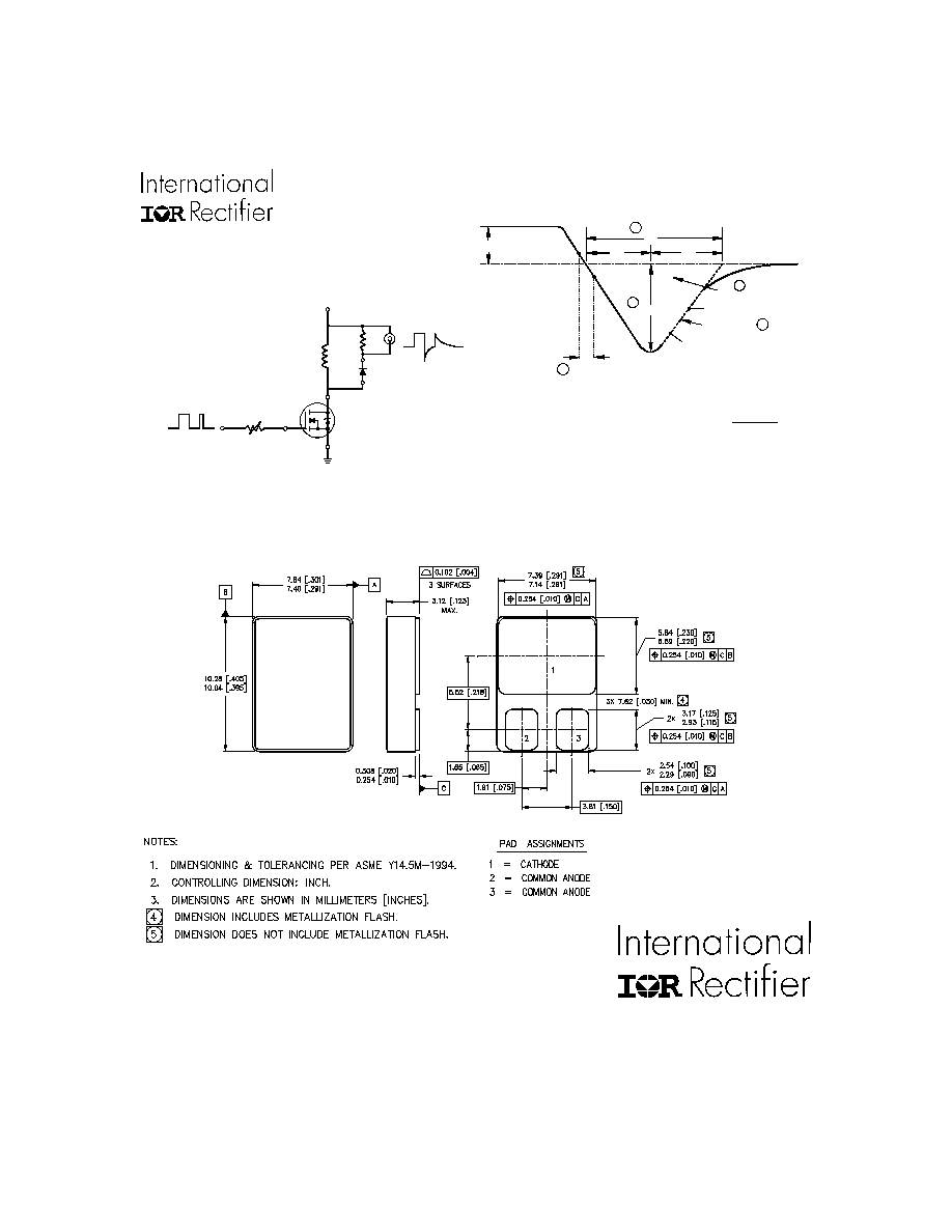
4. Q
rr
- Area under curve defined by t
rr
and I
RRM
t
rr
X I
RRM
Q
rr
=
2
5. di
(rec)M
/dt - Peak rate of change of
current during t
b
portion of t
rr
Fig. 10 - Reverse Recovery Waveform and Definitions
Fig. 9 - Reverse Recovery Parameter Test Circuit
t
a
t
b
t
rr
Q
rr
I
F
I
R R M
I
R R M
0 .5
d i(re c)M /d t
0.75 I
R R M
5
4
3
2
0
1
d i /d t
f
1. di
f
/dt - Rate of change of current
through zero crossing
2. I
RRM
- Peak reverse recovery current
3. trr - Reverse recovery time measured
from zero crossing point of negative
going I
F
to point where a line passing
through 0.75 I
RRM
and 0.50 I
RRM
extrapolated to zero current
R E V E R S E R E C O V E R Y C IR C U IT
IR F P 2 50
D .U .T .
L = 7 0 µ H
V = 2 00 V
R
0.01
G
D
S
d if/d t
A D JU S T
IR WORLD HEADQUARTERS: 233 Kansas St., El Segundo, California 90245, USA Tel: (310) 252-7105
TAC Fax: (310) 252-7903
Visit us at www.irf.com for sales contact information.
Data and specifications subject to change without notice. 07/01
Case Outline and Dimensions -- SMD-0.5