 | ÐлекÑÑоннÑй компоненÑ: HFB50HC20 | СкаÑаÑÑ:  PDF PDF  ZIP ZIP |
/home/web/doc/html/irf/172763
10/18/01
· Reduced RFI and EMI
· Reduced Snubbing
· Extensive Characterization of Recovery Parameters
· Hermetic
Features
Description
These Ultrafast, soft recovery diodes are optimized to reduce losses and EMI/RFI in high frequency power
conditioning systems. An extensive characterization of the recovery behavior for different values of current,
temperature and di/dt simplifies the calculations of losses in the operating conditions. The softness of the recovery
eliminates the need for a snubber in most applications. These devices are ideally suited for power converters, motors
drives and other applications where switching losses are significant portion of the total losses.
Ultrafast, Soft Recovery Diode
FRED
V
R
= 200V
I
F(AV)
= 50A
t
rr
= 35ns
Note:
Q
D.C. = 50% rect. wave
R
1/2 sine wave, 60 Hz , P.W. = 8.33 ms
HFB50HC20
www.irf.com
1
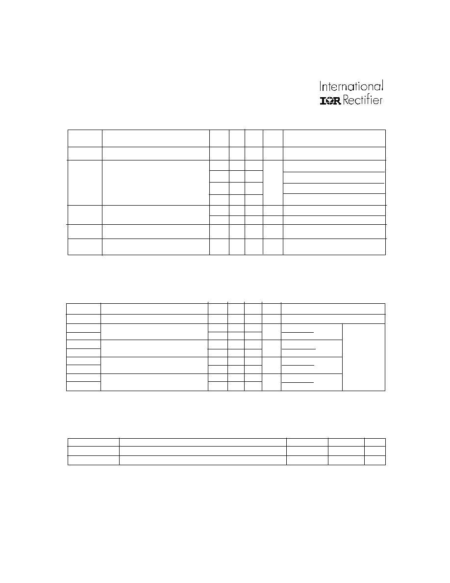
Parameter
Max.
Units
V
R
Cathode to Anode Voltage
200
V
I
F(AV)
Continuous Forward Current,
Q
T
C
= 87°C
50
I
FSM
Single Pulse Forward Current,
R
T
C
= 25°C
450
P
D
@ T
C
= 25°C
Maximum Power Dissipation
167
W
T
J,
T
STG
Operating Junction and Storage Temperature Range
-55 to +150
°C
A
Absolute Maximum Ratings
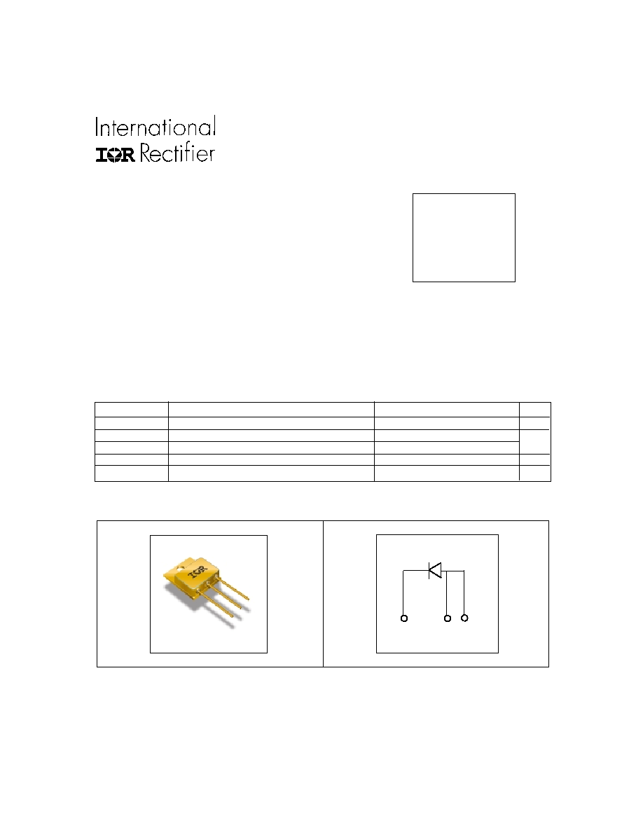
CASE STYLE
TO-258AA
ANODE
CATHODE
(ISOLATED BASE)
ANODE
PD - 94308A
2
www.irf.com
HFB50HC20
A/µs
nC
A
Dynamic Recovery Characteristics @ T
J
= 25°C (unless otherwise specified)
A/µs
nC
A
Parameter Min. Typ. Max. Units Test Conditions
t
rr
Reverse Recovery Time
--
--
35
ns
I
F
= 0.5A,V
R
= 30V, di
f
/dt = 300A/µs
t
rr1
Reverse Recovery Time
--
42
--
ns
T
J
= 25°C See Fig.
t
rr2
--
69
--
T
J
= 125°C 5
I
F
= 50A
I
RRM1
Peak Recovery Current
--
4.4
--
T
J
= 25°C See Fig.
I
RRM2
--
8.7
--
T
J
= 125°C 6
V
R
= 160V
Q
rr1
Reverse Recovery Charge
--
108
--
T
J
= 25°C See Fig.
Q
rr2
--
314 --
T
J
= 125°C 7
di
f
/dt = 200A/µs
di
(rec)M
/dt1
Peak Rate of Fall of Recovery Current
--
390
--
T
J
= 25°C See Fig.
di
(rec)M
/dt2
During t
b
--
570
--
T
J
= 125°C 8
Thermal - Mechanical Characteristics
Parameter
Typ.
Max.
Units
R
thJC
Junction-to-Case
--
0.75
Wt
Weight
10.9
--
g
°C/W
See Fig. 2
Parameter
Min. Typ. Max. Units
Test Conditions
V
BR
Cathode Anode Breakdown Voltage 200
--
-- V I
R
= 100µA
Electrical Characteristics @ T
J
= 25°C (unless otherwise specified)
L
S
Series Inductance
--
8.7
--
nH
Measured from anode lead to cathode
lead, 6 mm ( 0.025 in ) from package
C
T
Junction Capacitance, See Fig. 3
--
--
360
pF
V
R
= 200V
I
R
Reverse Leakage Current
--
--
10
µA
V
R
= V
R
Rated
See Fig. 2
--
--
200
µA
V
R
= V
R
Rated, T
J
= 125°C
V
F
Forward Voltage
--
-- 1.34
I
F
= 50A, T
J
= -55°C
See Fig. 1
--
-- 1.28
I
F
= 50A, T
J
= 25°C
-- -- 1.7
I
F
= 100A, T
J
= 25°C
-- -- 1.69
I
F
= 100A, T
J
= 125°C
V
S
S
T
T
T
T
Pulse Width < 300µs, Duty Cycle < 2%
Pins 2 and 3 externally tied together
S
T
Note:
www.irf.com
3
HFB50HC20
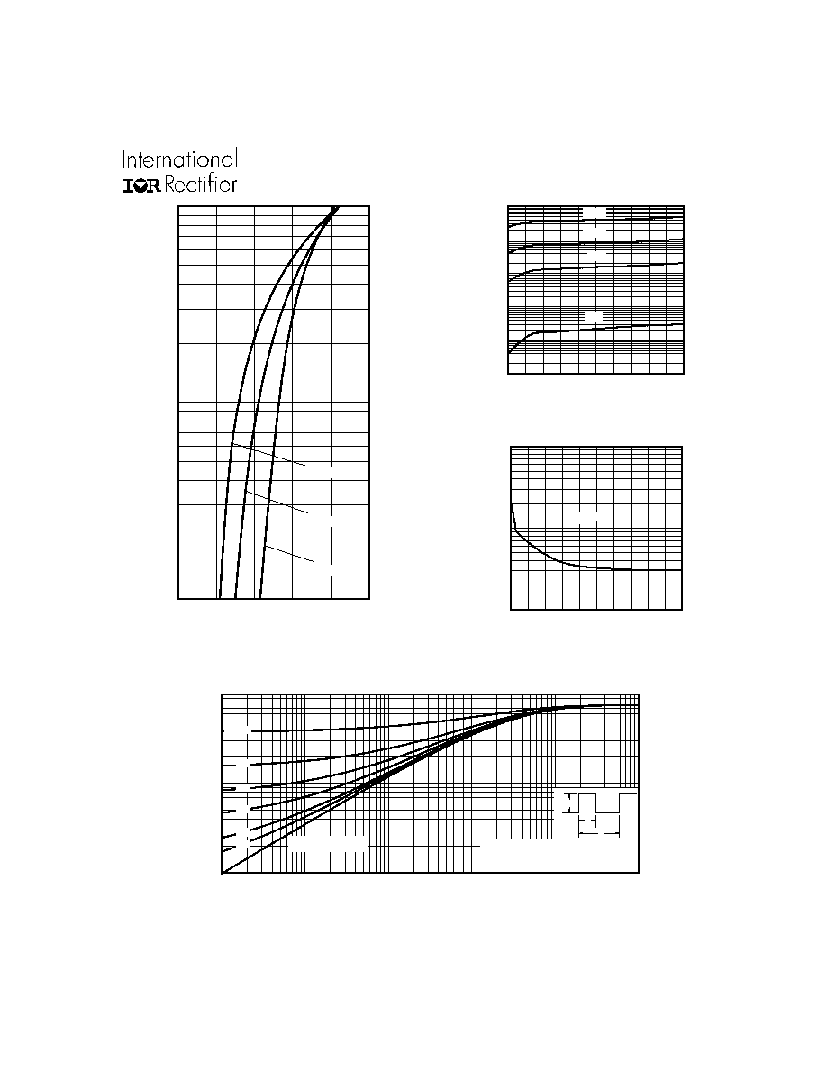
Fig. 4 - Maximum Thermal Impedance Z
thjc
Characteristics
Fig. 2 - Typical Reverse Current Vs. Reverse
Voltage
Fig. 3 - Typical Junction Capacitance Vs.
Reverse Voltage
Fig. 1 - Maximum Forward Voltage Drop Vs.
Instantaneous Forward Current
0
40
80
120
160
200
Reverse Voltage - VR (V)
100
1000
10000
Junction Capacitance - C
T
(pF)
TJ = 25°C
0.0
0.4
0.8
1.2
1.6
2.0
Forward Voltage Drop - V F (V)
1
10
100
Instantaneous Forward Current - I
F
(A)
Tj = -55°C
Tj = 125°C
Tj = 25°C
0
40
80
120
160
200
Reverse Voltage - V R (V)
0.001
0.01
0.1
1
10
100
Reverse Current - I
R
(µA)
125°C
75°C
25°C
100°C
0.01
0.1
1
0.00001
0.0001
0.001
0.01
0.1
1
Notes:
1. Duty factor D = t / t
2. Peak T = P
x Z
+ T
1
2
J
DM
thJC
C
P
t
t
DM
1
2
t , Rectangular Pulse Duration (sec)
Thermal Response
(Z )
1
thJC
0.01
0.02
0.05
0.10
0.20
D = 0.50
SINGLE PULSE
(THERMAL RESPONSE)
4
www.irf.com
HFB50HC20
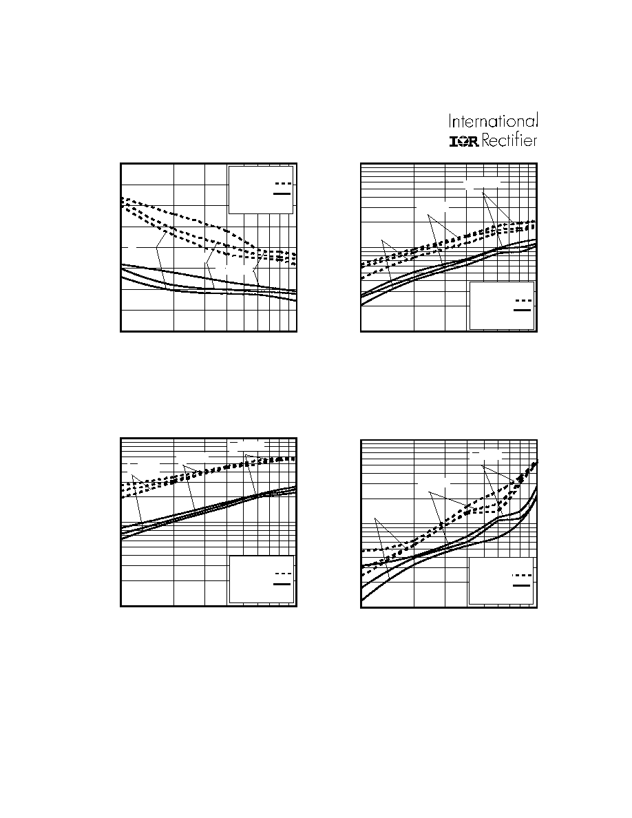
Fig. 7 - Typical Stored Charge Vs. di
f
/dt
Fig. 8 - Typical di
(rec)M
/dt Vs. di
f
/dt
Fig. 5 - Typical Reverse Recovery Vs. di
f
/dt,
Fig. 6 - Typical Recovery Current Vs. di
f
/dt,
100
1000
dif / dt - ( A / µs )
10
100
1000
Q
rr
- ( nC )
VR = 160V
TJ = 125°C
TJ = 25°C
IF = 25A
IF = 100A
IF = 50A
100
1000
dif / dt - ( A / µs )
100
1000
10000
di
( rec )M
/ dt - ( A / µs )
VR = 160V
TJ = 125°C
TJ = 25°C
IF = 25A
IF = 100A
IF = 50A
100
1000
dif / dt - ( A / µs )
1
10
100
I RRM
- ( A )
VR = 160V
TJ = 125°C
TJ = 25°C
IF = 25A
IF = 100A
IF = 50A
100
1000
dif / dt - ( A / µs )
20
40
60
80
100
t rr
- ( ns )
VR = 160V
TJ = 125°C
TJ = 25°C
IF = 25A
IF = 100A
IF = 50A
www.irf.com
5
HFB50HC20
4. Q
rr
- Area under curve defined by t
rr
and I
RRM
t
rr
X I
RRM
Q
rr
=
2
5. di
(rec)M
/dt - Peak rate of change of
current during t
b
portion of t
rr
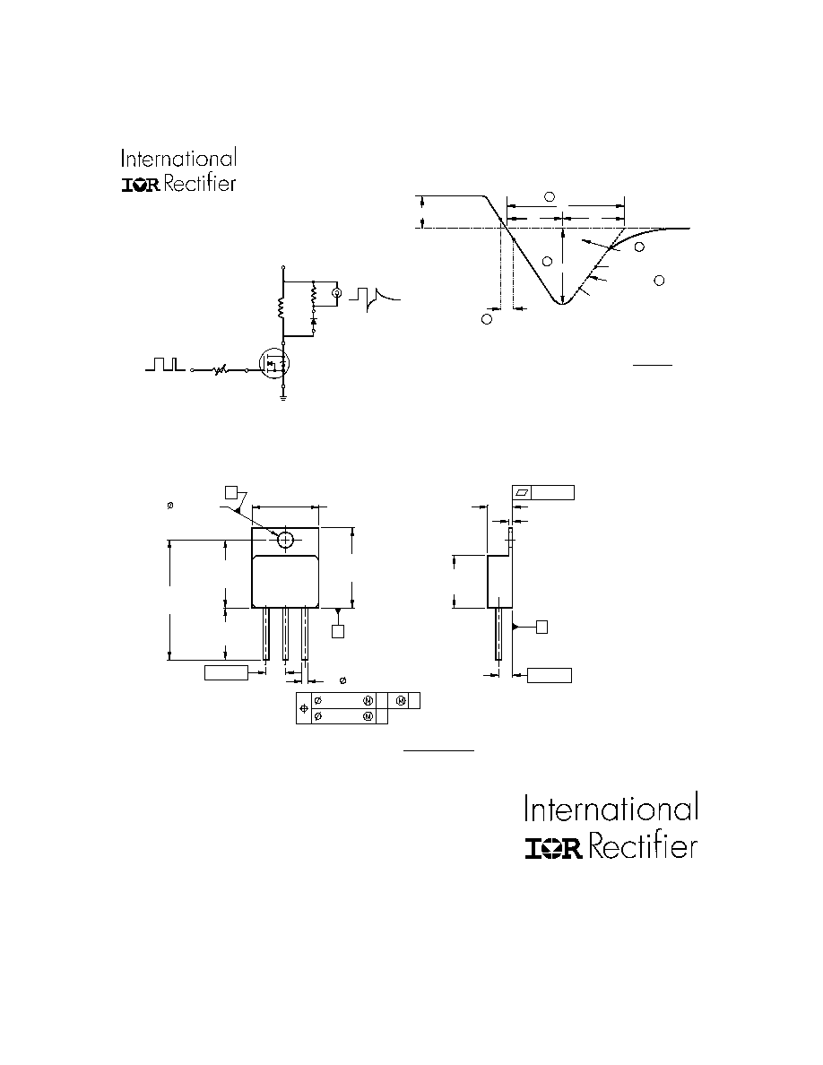
Fig. 10 - Reverse Recovery Waveform and Definitions
Fig. 9 - Reverse Recovery Parameter Test Circuit
t
a
t
b
t
rr
Q
rr
I
F
I
R R M
I
R R M
0 .5
d i(re c)M /d t
0.75 I
R R M
5
4
3
2
0
1
d i /d t
f
1. di
f
/dt - Rate of change of current
through zero crossing
2. I
RRM
- Peak reverse recovery current
3. trr - Reverse recovery time measured
from zero crossing point of negative
going I
F
to point where a line passing
through 0.75 I
RRM
and 0.50 I
RRM
extrapolated to zero current
R E V E R S E R E C O V E R Y C IR C U IT
IR F P 2 50
D .U .T .
L = 7 0 µ H
V = 2 00 V
R
0.01
G
D
S
d if/d t
A D JU S T
IR WORLD HEADQUARTERS: 233 Kansas St., El Segundo, California 90245, USA Tel: (310) 252-7105
TAC Fax: (310) 252-7903
Visit us at www.irf.com for sales contact information.
Data and specifications subject to change without notice. 10/01
Case Outline and Dimensions -- TO-258AA
PIN AS S IGNMENT S
1 = CATHODE
2 = ANODE
3 = ANODE
2
3
1
3X
2X
3.55 [.140]
13.97 [.550]
13.46 [.530]
B
0.12 [.005]
1.14 [.045]
0.88 [.035]
6.85 [.270]
6.09 [.240]
21.20 [.835]
20.70 [.815]
17.65 [.695]
17.39 [.685]
4.19 [.165]
3.93 [.155]
0.50 [.020]
C A
B
0.25 [.010]
C
37.00 [1.457]
20.40 [1.197]
17.95 [.707]
17.70 [.697]
19.05 [.750]
12.70 [.500]
1.65 [.065]
1.39 [.055]
C
5.08 [.200]
A
NOT ES :
1. DIMENS IONING & T OLERANCING PER AS ME Y14.5M-1994.
2. ALL DIMENS IONS ARE S HOWN IN MILLIMET ERS [INCHES ].
3. CONT ROLLING DIMENS ION: INCH.
4. CONFORMS T O JEDEC OUT LINE T O-258AA.