 | ÐлекÑÑоннÑй компоненÑ: iP1201TR | СкаÑаÑÑ:  PDF PDF  ZIP ZIP |
iP1201Final.PMD
· 3.14V to 5.5V input voltage
· 0.8V to 3.3V output voltage
· 2 Phase Synchronous Buck Power Block
· 180
°
out of phase operation
· Single or Dual output capability
· Dual 15A maximum load capability
· Single 2 phase 30A maximum load capability
· 200-400kHz per channel nominal switching frequency
· Over Current Hiccup or Over Current Latch
· External Synchronization capability
· Overvoltage protection
· Independent soft start per output
· Over Temperature protection
· Internal features minimize layout sensitivity *
· Very small outline 15.5mm x 9.25mm x 2.6mm
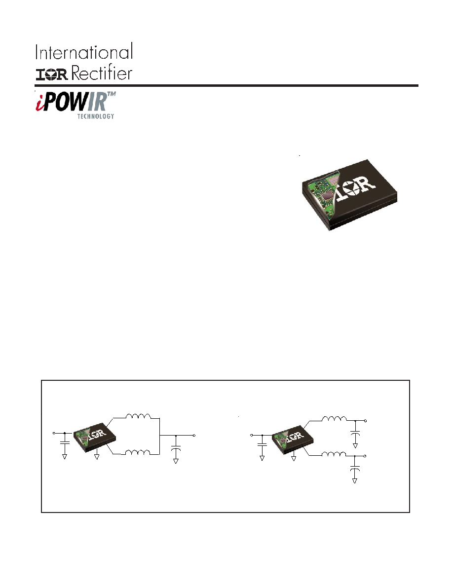
Dual Output Full Function 2 Phase
Synchronous Buck Power Block
Integrated Power Semiconductors,
PWM Control & Passives
The iP1201 is a fully optimized solution for medium current synchronous buck applications requiring up to 15A
or 30A. The iP1201 is optimized for 2 phase single output applications up to 30A or dual output, each up to
15A with interleaved input. It includes full function PWM control, with optimized power semiconductor chip-sets
and associated passives, achieving high power density. Very few external components are required to create
a complete synchronous buck power supply.
iPOWIR technology offers designers an innovative space-saving solution for applications requiring high power
densities. iPOWIR technology eases design for applications where component integration offers benefits in
performance and functionality. iPOWIR technology solutions are also optimized internally for layout, heat
transfer and component selection.
Description
iP1201 Power Block
Features
* Although, all of the difficult PCB layout and bypassing issues have been addressed with the internal design of the iPOWIR block, proper layout techniques should be applied
for the design of the power supply board. There are no concerns about unwanted shutdowns common to switching power supplies, if operated as specified. The iPOWIR block
will function normally, but not optimally without any additional input decoupling capacitors. Input decoupling capacitors should be added at Vin pin for stable and reliable long
term operation. See layout guidelines in datasheet for more detailed information.
PD-94590
10/6/03
iP1201
www.irf.com
1
iP1201 Configurations
Dual Output
Single Output
V
IN
V
OUT
V
IN
V
OUT
Channel 1
Channel 2
V
OUT
Channel 1
Channel 2
V
IN
V
OUT
Channel 1
Channel 2
V
OUT
Channel 1
Channel 2
V
IN
V
OUT
www.irf.com
2
iP1201
Absolute Maximum Ratings
Recommended Operating Conditions
Electrical Specifications @ V
IN
= 5V
All specifications @ 25°C (unless otherwise specified)
Parameter
Symbol
Min
Typ
Max
Units
Conditions
Input Voltage Range
V
IN
3.14
-
5.5
-
-
15
A
2 Independent outputs
T
PCB
= T
CASE
= 90°C. See Fig. 3
-
-
11.5
A
2 Independent outputs
T
PCB
= 90°C, T
CASE
= no airflow, no
heatsink. See Fig. 3
0.8
-
3.3
For V
IN
= 5V
0.8
-
2.5
For V
IN
= 3.3V
Output Voltage Range
V
OUT
V
Output RMS Current Per Channel
Iout
VSW
Parameter
Symbol
Min
Typ
Max
Units
Conditions
V
IN
V
IN
-0.3
-
5.8
Feedback
VFB1/VFB2
-0.3
-
6
Output Overvoltage Sense
VFB1
S
/VFB2
S
-0.3
-
6
PGOOD
-0.3
-
6
ENABLE
-0.3
-
5.8
Soft Start
SS1/SS2
-0.3
-
6
Vp-ref
-0.3
-
6
HICCUP
HICCUP
-0.3
-
6
SYNC
-0.3
-
6
Output RMS Current Per Channel
Iout
VSW
-
-
15
A
2 Independent outputs. See Fig. 3
Block Temperature
T
BLK
-40
-
125
°C
Capable of start up over full
temperature range. See Note 1.
V
Parameter
Symbol
Min
Typ
Max
Units
Conditions
Over Current Shutdown
I
OC
-
20
-
A
V
IN
= 5V, V
OUT
= 1.5V,
f
SW
= 300KHz, HICCUP pin pulled
Low
HICCUP duty cycle
D
HICCUP
-
5
-
%
HICCUP pin pulled high, output
short circuited.
Soft Start Time
t
SS
-
5
-
ms
V
IN
= 5V, V
OUT
= 1.5V,
C
SS1
= C
SS2
= 0.1
µ
F
Reference Voltage
V
REF
-
0.80
-
V
I
OUT
= 2A
V
OUT_ACC1
-3
-
3
T
BLK
= -40°C to 125°C, See Note 1.
V
IN
= 5V, V
OUT
= 1.5V
V
OUT_ACC2
-2.5
-
2.5
T
BLK
= 0°C to 125°C, See Note 1.
V
IN
= 5V, V
OUT
= 1.5V
Error Ampifier 1 & 2 input offset
voltage
V
OS1
, V
OS2
-4
-
4
mV
V
IN
= 5V, V
OUT
= 1.5V
FB1 / FB2 Input bias current
I
B1
, I
B2
-
-0.1
-
µ
A
Error Amplifier
source/sink Current
I
ERR
-
60
-
µ
A
Error Amplifier
Transconductance
g
m1,
g
m2
-
2000
-
µ
mho
Output Overvoltage Shutdown
Threshold
OVP
-
1.15 x V
OUT
-
V
See OVP note in Design Guidelines
OVP Fault Propagation Delay
t
OVP
-
25
-
µ
s
Output forced to 1.125Vref
PGOOD Trip Threshold
V
Th_PGOOD
-
0.85 x V
OUT
-
V
FB1 or FB2 ramping down
PGOOD Output Low Voltage
V
Lo_PGOOD
-
0.25
-
V
I
SINK
= 2mA
%
V
OUT
Accuracy
W
P
LOSS
Power Loss
f
SW =
300kHz, V
IN
= 5V, V
OUT
= 1.5V,
I
OUT
= 15A
-
6.7
8.4
www.irf.com
3
iP1201
Electrical Specifications (continued)
Note 1: Guaranteed to meet specifications from T
BLK
= 0°C to 90°C. Specifications outside of this temperature range are
guaranteed by design, and not production tested.
Parameter
Symbol
Min
Typ
Max
Units
Conditions
Frequency
f
SW
255
-
345
kHz
R
T
set to 30.9k
Sync Frequency Range
f
SYNC
480
-
800
kHz
Free running frequency
set 20% below sync frequency
Sync Pulse Duration
t
SYNC
-
200
-
ns
Sync, Hiccup High Level
Threshold Voltage
2
-
-
V
Sync, Hiccup Low Level
Threshold Voltage
-
-
0.8
V
V
IN
Quiescent Current
I
IN_Leakage
-
1.0
-
mA
V
IN
= 5V, Enable high
Thermal Shutdown
Temp
shdn
-
140
-
°C
Max Duty Cycle
D
MAX
90
-
-
%
f
SW
= 200kHz
Enable Input Logic High
V
EN-Hi
2
-
-
V
V
IN
= V
MIN
to V
MAX
Enable Input Logic Low
V
EN-Lo
-
-
0.4
V
V
IN
= V
MIN
to V
MAX
V
IN
Undervoltage Lockout
Threshold Voltage
V
IN_UVLO
-
2.7
-
V
V
IN
= 5V, ENABLE Pulled Low
Output Disable Soft Start Low
Threshold Voltage
V
SS_Dis
-
-
0.25
V
SS1 / SS2 Pins Pulled Low
www.irf.com
4
iP1201
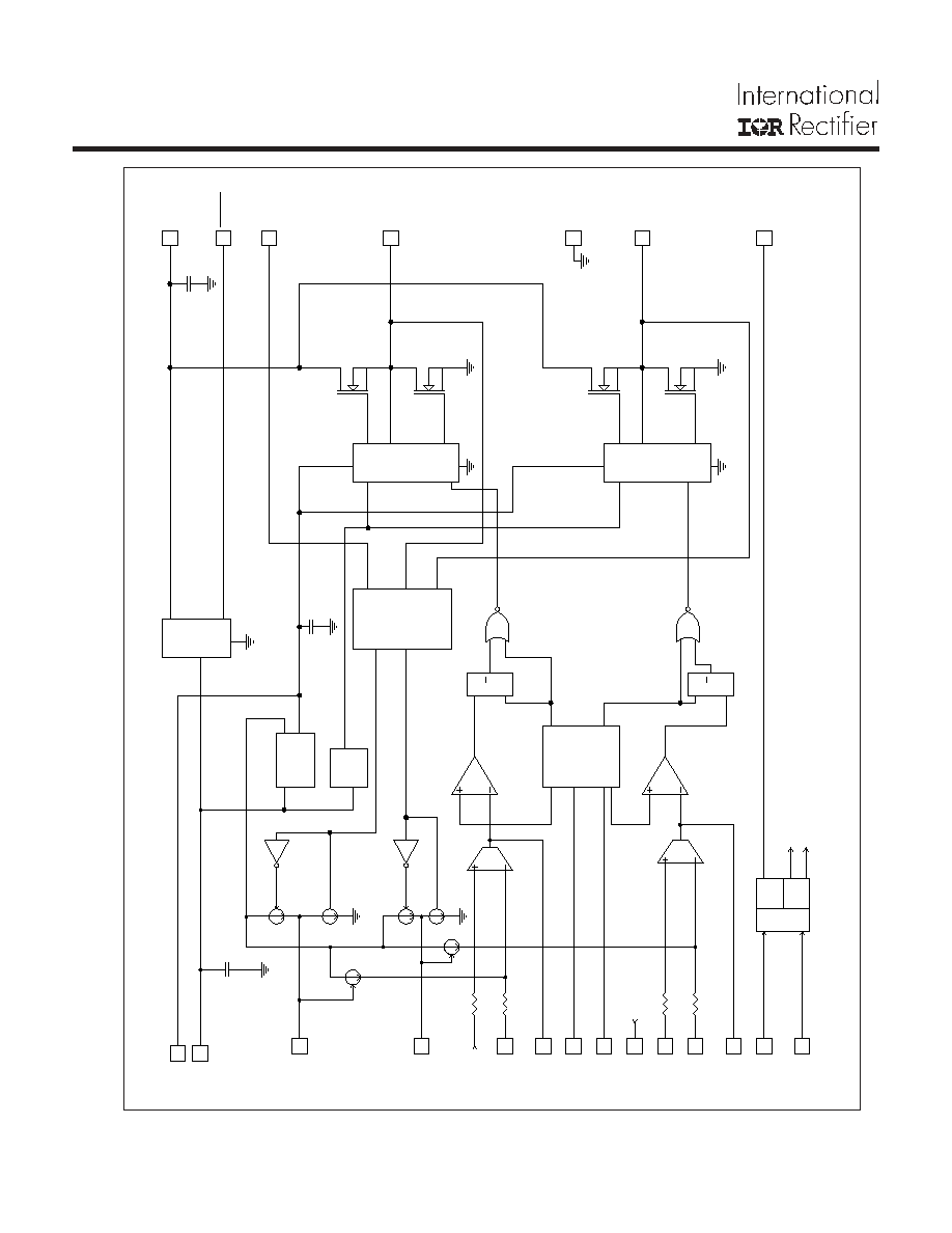
H
i
ccup
Co
n
t
ro
l
OC
L
a
t
c
h
/
PG
ood
OVP
(
-
10%
)
(
+
15%
)
Bias
Gen
erat
o
r
SS1
SS2
H
I
CCU
P
FB1
CC1
SYNC
RT
VR
EF
VP-R
E
F
FB2
CC2
FB1
S
FB2
S
25uA
25uA
25k
25k
25k
25k
E
r
ror A
m
p1
E
rror A
m
p2
0.8V
T
w
o ph
a
s
e
Osci
l
l
at
o
r
PW
M
C
o
m
p
1
PW
M
C
o
m
p
2
R
S
Q
R
S
Q
Ra
m
p
1
Ra
m
p
2
SW
1
/ SW
3
OF
F
SW
2
/ SW
4
ON
ENAB
L
E
PGOOD
VSW
1
SW
2
SW
1
SW
4
SW
3
0.8V
VC
C
VSW
2
UVL
O
3uA
3uA
VIN
Dr
i
v
er
1
Dr
i
v
er
2
PW
M
1
PW
M
2
B
A
D
o
ubl
e
r
PGND
64uA
64uA
Fig. 1:
iP1201 Internal Block Diagram
www.irf.com
5
iP1201
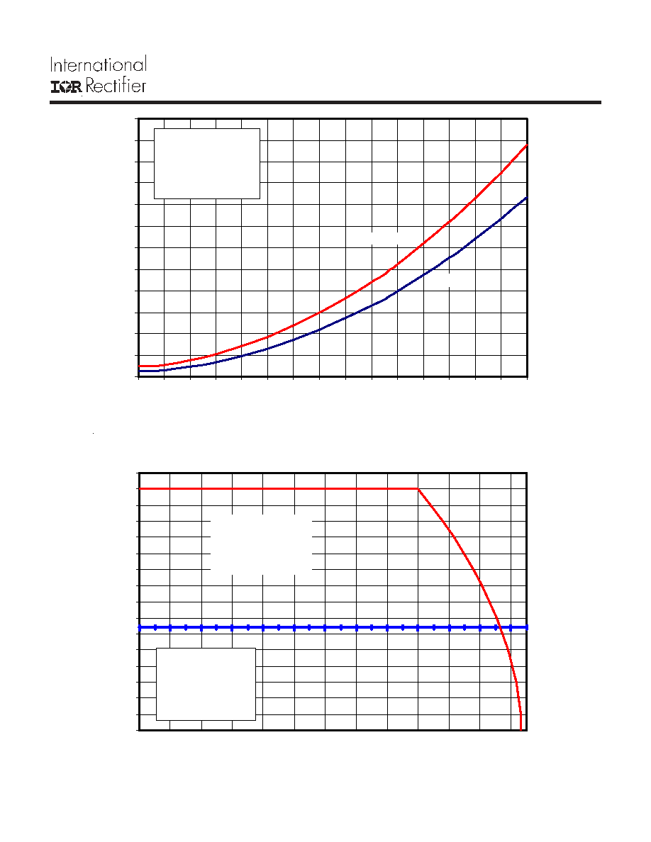
Fig. 2: Power Loss vs. Current
Fig. 3: Safe Operating Area (SOA) vs. T
PCB
& T
CASE
0
10
20
30
40
50
60
70
80
90
100
120
110
0
1
2
3
4
5
6
7
8
9
10
11
12
13
14
15
16
0
10
20
30
40
50
60
70
80
90
100
110
120
PCB Te m pe rature (ºC)
O
u
t
put
C
u
r
r
e
n
t
P
e
r
C
h
a
nne
l
(
A
)
Cas e Te m pe r atur e (
&�
T
X
V
IN
= 5V
V
OUT 1
= V
OUT 2
= 1.5V
I
OUT
= 15A
f
SW
= 300kHz
L = 1.8uH
Safe
Operating
Area
0
1
2
3
4
5
6
7
8
9
10
11
12
0
1
2
3
4
5
6
7
8
9
10
11
12
13
14
15
Output Current Per Channel (A)
T
o
t
a
l
P
o
w
e
r
L
o
ss
,
Bo
th
O
u
tp
u
t
s
(
W
)
V
IN
= 5V
V
OUT 1
= V
OUT 2
= 1.5V
f
SW
= 300kHz
L = 1.8
µ
H
T
BLK
= 125°C
Maximum
T ypical