 | ÐлекÑÑоннÑй компоненÑ: IPS041L | СкаÑаÑÑ:  PDF PDF  ZIP ZIP |
Äîêóìåíòàöèÿ è îïèñàíèÿ www.docs.chipfind.ru
Features
·
Over temperature shutdown
·
Over current shutdown
·
Active clamp
·
Low current & logic level input
·
E.S.D protection
IPS041L
FULLY PROTECTED POWER MOSFET SWITCH
Data Sheet No.PD 60152-K
Description
The IPS041L is a fully protected three terminal SMART
POWER MOSFET that features over-current, over-
temperature, ESD protection and drain to source
active clamp.This device combines a HEXFET®
POWER MOSFET and a gate driver. It offers full
protection and high reliability required in harsh envi-
ronments. The driver allows short switching times
and provides efficient protection by turning OFF the
power MOSFET when the temperature exceeds 165
o
C
or when the Drain current reaches 2A. The device
restarts once the input is cycled. The avalanche
capability is significantly enhanced by the active
clamp and covers most inductive load demagnetiza-
tions.
Package
Product Summary
R
ds(on)
500m
(max)
V
clamp
50V
I
shutdown
2A
T
on
/T
off
1.5
µ
s
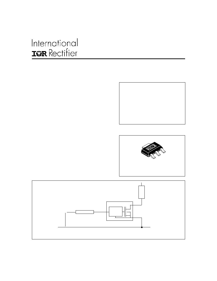
Typical Connection
3 Lead SOT223
www.irf.com
1
S
Q
Load
D
S
control
IN
R in series
(if needed)
Logic signal
(Refer to leads assignments for correct pin configuration)
IPS041L
2
www.irf.com
(1) Limited by junction temperature (pulsed current limited also by internal wiring)
(2) Operations at higher switching frequencies is possible. See Appl. notes.
Recommended Operating Conditions
These values are given for a quick design. For operation outside these conditions, please consult the application notes.
Symbol Parameter
Min.
Max. Units
Vds (max) Continuous drain to source voltage
--
35
VIH
High level input voltage
4
6
VIL
Low level input voltage
0
0.5
Ids
Continuous drain current
Tamb=85
o
C
(TAmbient = 85
o
C, IN = 5V, rth = 100
o
C/W, Tj = 125
o
C)
--
0.75
A
Rin
Recommended resistor in series with IN pin
1
5
k
Tr-in(max) Max recommended rise time for IN signal (see fig. 2)
--
1
µ
S
Fr-Isc
(2)
Max. frequency in short circuit condition (Vcc = 14V)
0
1
kHz
V
Absolute Maximum Ratings
Absolute maximum ratings indicates sustained limits beyond which damage to the device may occur. All voltage parameters are
referenced to SOURCE lead. (TAmbient = 25
o
C unless otherwise specified). PCB mounting uses the standard footprint with 70
µ
m
copper thickness.
Symbol Parameter
Min.
Max.
Units
Test Conditions
Vds
Maximum drain to source voltage
--
47
Vin
Maximum input voltage
-0.3
7
Iin, max
Maximum IN current
-10
+10
mA
Isd
cont.
Diode max. continuous current
(1)
(rth=125
o
C/W)
--
1.2
Isd
pulsed
Diode max. pulsed current
(1)
--
3
Pd
Maximum power dissipation
(1)
(rth=125
o
C/W)
--
1
W
ESD1
Electrostatic discharge voltage
(Human Body)
--
4
C=100pF, R=1500
,
ESD2
Electrostatic discharge voltage
(Machine Model)
--
0.5
C=200pF, R=0
,
L=10
µ
H
T stor.
Max. storage temperature
-55
150
Tj max.
Max. junction temperature
-40
150
o
C
V
A
kV
o
C
Thermal Characteristics
Symbol Parameter
Min.
Typ.
Max. Units Test Conditions
Rth
1
Thermal resistance with standard footprint
--
100
--
Rth
2
Thermal resistance with 1" square footprint
--
60
--
o
C/W
IPS041L
www.irf.com
3
Symbol Parameter
Min.
Typ.
Max. Units Test Conditions
Tsd
Over temperature threshold
--
165
--
o
C
See fig. 1
Isd
Over current threshold
1.1
1.7
2.2
A
See fig. 1
V
reset
IN protection reset threshold
1.5
2.3
3
V
Treset
Time to reset protection
2
10
40
µ
s Vin = 0V, Tj = 25
o
C
EOI_OT
Short circuit energy (see application note)
--
400
--
µ
J
Vcc = 14V
Protection Characteristics
Symbol Parameter
Min.
Typ.
Max. Units Test Conditions
Rds(on)
ON state resistance Tj = 25
o
C
--
370
500
Tj = 150
o
C
--
590
900
Idss1
Drain to source leakage current
0
0.5
25
Vcc = 14V, Tj = 25
o
C
@Tj=25
o
C
Idss2
Drain to source leakage current
0
5
50
Vcc = 40V, Tj = 25
o
C
@Tj=25
o
C
V
clamp 1
Drain to Source clamp voltage 1
47
52
56
Id = 20mA
(see Fig.3 & 4)
V
clamp 2
Drain to Source clamp voltage 2
50
53
60
Vin
clamp
IN to Source clamp voltage
7
8.1
9.5
Iin = 1 mA
Vin th
IN threshold voltage
1
1.6
2
Id = 50mA, Vds = 14V
Iin, -on
ON state IN positive current
25
90
200
Vin = 5V
Iin, -off
OFF state IN positive current
50
130
250
Vin = 5V
over-current triggered
Static Electrical Characteristics
(Tj = 25
o
C unless otherwise specified.)
m
Vin = 5V, Ids = 1A
Id=Ishutdown
(see Fig.3 & 4)
V
µ
A
Switching Electrical Characteristics
Vcc = 14V, Resistive Load = 20
, Rinput = 1k
,
100
µ
s
pulse, T
j
= 25
o
C, (unless otherwise specified).
Symbol Parameter
Min.
Typ.
Max. Units Test Conditions
Ton
Turn-on delay time
0.05
0.2
0.5
Tr
Rise time
0.5
1.3
2.5
Trf
Time to 130% final Rds(on)
--
5
--
Toff
Turn-off delay time
0.5
1.6
2.5
Tf
Fall time
0.5
1.5
2.5
Qin
Total gate charge
--
1
--
nC
Vin = 5V
See figure 2
See figure 2
µ
s
µ
A
IPS041L
4
www.irf.com
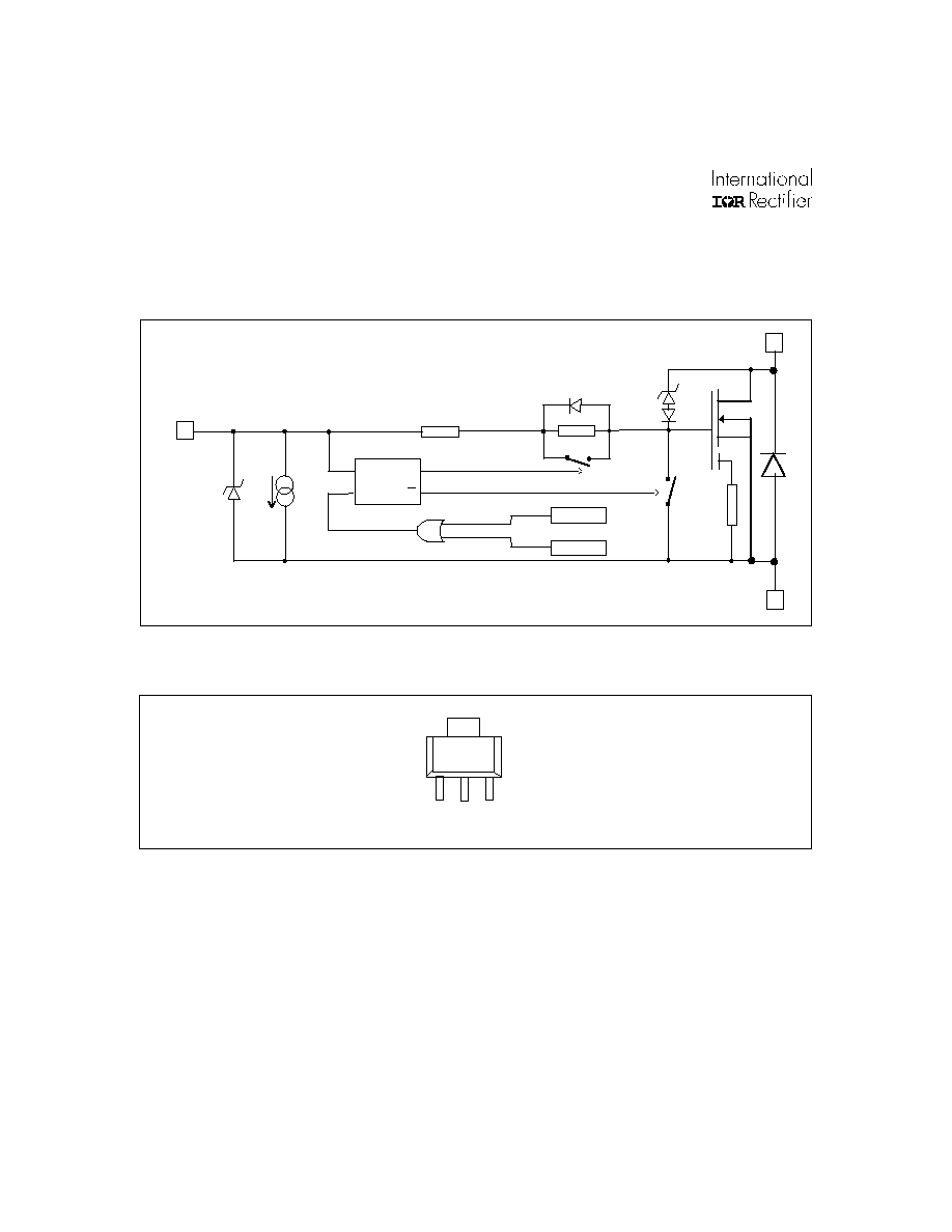
Lead Assignments
(2) D
1 2 3
In D S
Functional Block Diagram
All values are typical
IN
DRAIN
SOURCE
8.1 V
80
µ
A
47 V
I sense
200 k
4000
S
Q
R
Q
T > 165°c
I > 1sd
IPS041L
www.irf.com
5
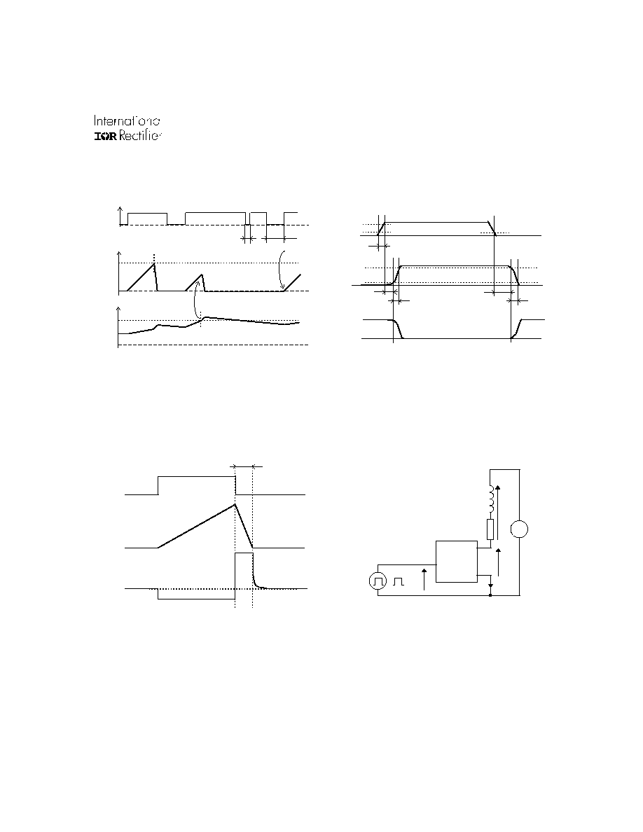
Figure 1 - Timing diagram
Tr-in
10 %
90 %
90 %
10 %
Td on
Td off
tf
tr
Ids
Tr-in
Vin
Vds
Figure 2 - IN rise time & switching time definitions
Tsd
(165 °c)
Vin
Ids
Isd
I shutdown
T
T shutdown
t < T reset
t > T reset
5 V
0 V
14 V
IN
D
S
5 v
0 v
L
R
+
-
Vds
Ids
Vin
V load
Rem : V load is negative
during demagnetization
Figure 4 - Active clamp test circuit
Ids
Vds
Vin
T clamp
Vds clamp
( Vcc )
( see Appl . Notes to evaluate power dissipation )
Figure 3 - Active clamp waveforms