 | ÐлекÑÑоннÑй компоненÑ: IPS521S | СкаÑаÑÑ:  PDF PDF  ZIP ZIP |
Äîêóìåíòàöèÿ è îïèñàíèÿ www.docs.chipfind.ru
Features
·
Over temperature protection (with auto-restart)
·
Short-circuit protection (current limit)
·
Active clamp
·
E.S.D protection
·
Status feedback
·
Open load detection
·
Logic ground isolated from power ground
IPS521/IPS521S
Data Sheet No.PD 60158-H
Description
The IPS521/IPS521S are fully protected five terminal
high side switches with built in short-circuit , over-
temperature, ESD protection, inductive load capability
and diagnostic feedback. The output current is con-
trolled when it reaches Ilim value. The current
limitation is activated until the thermal protection
acts. The over-temperature protection turns off the
high side switch if the junction temperature exceeds
Tshutdown. It will automatically restart after the junc-
tion has cooled 7
o
C below Tshutdown. A diagnostic
pin is provided for status feedback of short-circuit,
over-temperature and open load detection. The double
level shifter circuitry allows large offsets between the
logic ground and the load ground.
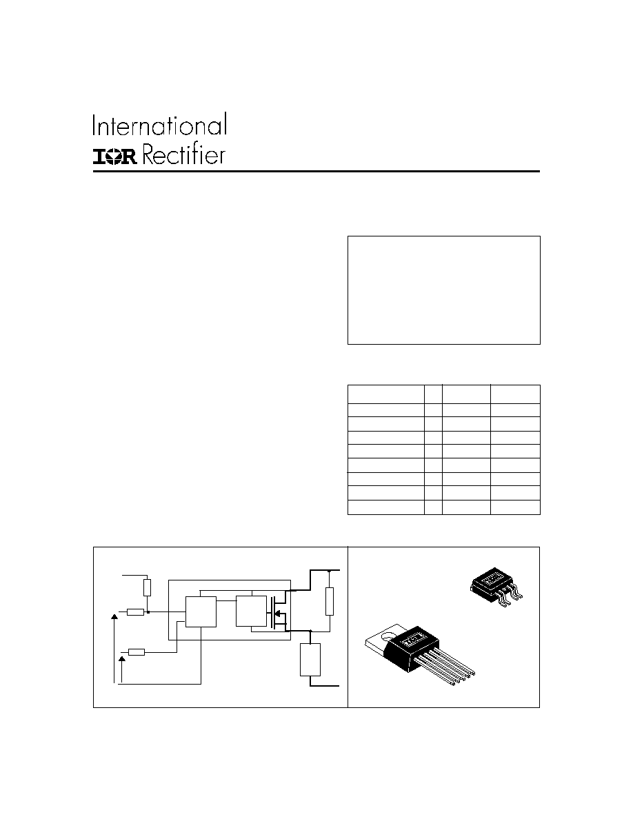
Packages
Product Summary
R
ds(on)
80m
(max)
V
clamp
50V
I
Limit
10A
V
open load
3V
Typical Connection
FULLY PROTECTED HIGH SIDE POWER MOSFET SWITCH
5 Lead
TO220 - IPS521
5 Lead
D2Pak (SMD220)
IPS521S
Load
Logic
signal
control
Logic
Logic Gnd
Load Gnd
Vcc
Out
Gnd
In
Dg
+ 5v
Status
feedback
+ VCC
Output pull-up resistor
Rdg
Rin
15K
Truth Table
Op. Conditions
Normal
Normal
Open load
Open load
Over current
Over current
Over-temperature
Over-temperature
In
H
L
H
L
H
L
H
L
Out
H
L
H
H
L
L (cycling)
L
L (limiting)
Dg
H
L
H
H
L
L
L
L
www.irf.com
1
IPS521/IPS521S
2
www.irf.com
(1) Limited by junction temperature (pulsed current limited also by internal wiring)
Symbol Parameter
Min.
Typ.
Max. Units Test Conditions
Rth 1
Thermal resistance junction to case
--
!
--
Rth 2
Thermal resistance junction ambient
--
$
--
Rth 1
Thermal resistance with standard footprint
--
60
--
Rth 2
Thermal resistance with 1" square footprint
--
35
--
Rth 3
Thermal resistance junction to case
--
!
--
Thermal Characteristics
TO-220
D
2
PAK (SMD220)
o
C/W
Absolute Maximum Ratings
Absolute maximum ratings indicate sustained limits beyond which damage to the device may occur. All voltage parameters
are referenced to GROUND lead. (Tj = 25
o
C unless otherwise specified).
Symbol Parameter
Min.
Max.
Units
Test Conditions
Vout
Maximum output voltage
Vcc-50 Vcc+0.3
Voffset
Maximum logic ground to load ground offset Vcc-50 Vcc+0.3
Vin
Maximum Input voltage
-0.3
7
Iin, max
Maximum positive IN current
-5
10
mA
Vdg
Maximum diagnostic output voltage
-0.3
7
V
Idg, max
Maximum diagnostic output current
-1
10
mA
Isd
cont.
Diode max. permanent current
(1)
(rth=62
o
C/W)
--
2.2
Isd
pulsed
Diode max. pulsed current
(1)
--
10
ESD1
Electrostatic discharge voltage
(Human Body)
--
4
C=100pF, R=1500
,
ESD2
Electrostatic discharge voltage
(Machine Model)
--
0.5
C=200pF, R=0
,
L=10
µ
H
Pd
Maximum power dissipation
(1)
(TC=25
o
C) IPS521
--
40
(TC=25
o
C) IPS521S
--
1.56
Tj max.
Max. storage & operating junction temp.
-40
+150
Tlead
Lead temperature (soldering 10 seconds)
--
300
Vcc max. Maximum Vcc voltage
--
50
V
V
A
kV
W
o
C
IPS521/IPS521S
www.irf.com
3
Recommended Operating Conditions
These values are given for a quick design. For operation outside these conditions, please consult the application notes.
Symbol Parameter
Min.
Max. Units
Vcc
Continuous Vcc voltage
5.5
35
VIH
High level input voltage
4
5.5
VIL
Low level input voltage
-0.3
0.9
Iout
Continuous output current
(Tamb = 85
o
C, Tj = 125
o
C, Rth = 60
o
C/W, ) IPS521
--
2.2
Iout
Continuous output current
(Tamb = 85
o
C, Tj = 125
o
C, Rth = 80
o
C/W, ) IPS521S
--
1.9
Rin
Recommended resistor in series with IN pin
4
6
Rdg
Recommended resistor in series with DG pin
10
20
V
A
k
Symbol Parameter
Min.
Typ.
Max. Units Test Conditions
Rds(on)
ON state resistance Tj = 25
o
C
--
55
80
@Tj=25
o
C
Rds(on)
ON state resistance @ Vcc = 6V
--
55
80
(Vcc=6V)
Rds(on)
ON state resistance Tj = 150
o
C
--
110
140
Vin = 5V, Iout = 5A
@Tj=150
o
C
Vcc oper. Operating voltage range
5.5
--
35
V
clamp 1
Vcc to OUT clamp voltage 1
50
55
--
Id = 10mA
(see Fig.1 & 2)
V
clamp 2
Vcc to OUT clamp voltage 2
--
56
65
Vf
Body diode forward voltage
--
0.9
1.2
Id = 2.5A, Vin = 0V
Icc off
Supply current when OFF
--
16
50
µ
A
Vin = 0V, Vout = 0V
Icc on
Supply current when ON
--
0.6
2
mA
Vin = 5V
Icc ac
Ripple current when ON (AC RMS)
--
20
--
µ
A
Vin = 5V
Vdgl
Low level diagnostic output voltage
--
0.15
0.4
V
Idg = 1.6 mA
Ioh
Output leakage current
--
50
120
Vout = 6V
Iol
Output leakage current
0
--
25
Vout = 0V
Idg
leakage
Diagnostic output leakage current
--
--
10
Vdg = 5.5V
Vih
IN high threshold voltage
--
2.2
3
Vil
IN low threshold voltage
1
1.9
--
Iin, on
On state IN positive current
--
70
200
µ
A
Vin = 5V
In hyst
Input hysteresis
0.1
0.25
0.5
V
Static Electrical Characteristics
(Tj = 25
o
C, Vcc = 14V unless otherwise specified.)
m
Vin = 5V, Iout = 5A
Id = Isd
(see Fig.1 & 2)
V
Vin = 5V, Iout = 2.5A
µ
A
V
IPS521/IPS521S
4
www.irf.com
Switching Electrical Characteristics
Vcc = 14V, Resistive Load = 2.8
, T
j
= 25
o
C, (unless otherwise specified).
Symbol Parameter
Min.
Typ.
Max. Units Test Conditions
Tdon
Turn-on delay time
--
10
40
Tr1
Rise time to Vout = Vcc - 5V
--
25
60
Tr2
Rise time Vcc - 5V to Vout = 90% of Vcc
--
130
200
dV/dt (on) Turn ON dV/dt
--
0.7
2
V/
µ
s
Eon
Turn ON energy
--
1500
--
µ
J
Tdoff
Turn-off delay time
--
35
70
Tf
Fall time to Vout = 10% of Vcc
-- 25
50
dV/dt (off) Turn OFF dV/dt
--
0.9
3
V/
µ
s
Eoff
Turn OFF energy
--
250
--
µ
J
Tdiag
Vout to Vdiag propagation delay
--
5
15
µ
s
See figure 6
See figure 3
µ
s
µ
s
See figure 4
Lead Assignments
Part Number
1 2 3 4 5
5 Lead - TO220
IPS521
3 (Vcc)
5 Lead - D
2
PAK (SMD220)
IPS521S
3 (Vcc)
1 2 3 4 5
1 - Ground
2 - In
3 - Vcc
4 - DG
5 - Out
(3) Referenced to Vcc
Symbol Parameter
Min.
Typ.
Max. Units Test Conditions
Ilim
Internal current limit
7
10
14
A
Vout = 0V
Tsd+
Over-temp. positive going threshold
--
165
--
See fig. 2
Tsd-
Over-temp. negative going threshold
--
158
--
See fig. 2
V
sc
Short-circuit detection voltage (3)
2
3
4
See fig. 2
V
open load
Open load detection threshold
2
3
4
Protection Characteristics
o
C
V
IPS521/IPS521S
www.irf.com
5
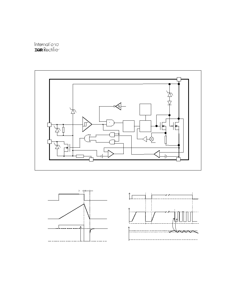
Functional Block Diagram
All values are typical
2.2 V
2.7 V
+
-
Level
shift
driver
Charge
pump
10 A
VCC
IN
50V
Over
Current
limit
VOUT
GND
DG
7 V
7 V
62 V
40
200 K
+
-
Open load
3 V
-
+
3 V
Tj
158°C
temperature
165°C
Short-circuit
Figure 1 - Active clamp waveforms
Figure 2 - Protection timing diagram
Tsd+
(160 ° )
Vin
Iout
Ilim.
T
5 V
0 V
Tsd-
T shutdown
limiting
cycling
T clamp
V clamp
( + Vcc )
( see Appl . Notes to evaluate power dissipation )
0 V
Vin
Iout
Out