 | –≠–ª–µ–∫—Ç—Ä–æ–Ω–Ω—ã–π –∫–æ–º–ø–æ–Ω–µ–Ω—Ç: IPS5551T | –°–∫–∞—á–∞—Ç—å:  PDF PDF  ZIP ZIP |

Features
∑
Over temperature shutdown
∑
Over current shutdown
∑
Active clamp
∑
Input referenced to + Vcc
∑
E.S.D protection
∑
Input referenced to Vcc
IPS5551T
FULLY PROTECTED HIGH SIDE POWER MOSFET SWITCH
Description
The IPS5551T is a fully protected three terminal high side
switch with built-in short-circuit, over-temperature, ESD
protection, inductive load capability. The input signal is
referenced to Vcc. When the input voltage Vcc - Vin is
higher than the specified threshold, the output power
MOSFET is turned on. When the Vcc - Vin is lower than the
specified Vil threshold, the output MOSFET is turned off.
Input noise immunity is improved by an hysterisis. When
the input is left floating, an internal current source pulls it up
to Vcc. The over-current protection latches off the high side
switch if the output current exceeds the specified Isd. The
over-temperature protection latches off the switch if the
junction temperature exceeds the specified value Tsd. The
device is reset by opening the input pin high.
Package
Product Summary
Rds(on)
6.0m
(max)
V clamp
40V
Ishutdown
100A
Vcc (op.)
5.5 - 18V
Typical Connection
Load
Input
signal
control
Logic
Vcc
Out
In
+ VCC
Op. Conditions
Normal
Normal
Over current
Over current
Over-temperature
Over-temperature
In
L
H
L
H
L
H
Out
H
L
L (latched)
L
L (latched)
L
Truth Table
(3)
Data Sheet No. PD60168-D
(3) In is referenced to Vcc.
In = L means (Vcc -Vin) >Vih
In = H means (Vcc - Vin) <Vil
SUPER TO220
www.irf.com
1
(Refer to lead assignment for correct pin configuration)

IPS5551T
2
www.irf.com
(1) Limited by junction temperature. Pulsed current is also limited by wiring
Absolute Maximum Ratings
Absolute maximum ratings indicate sustained limits beyond which damage to the device may occur. All voltage pa-
rameters are referenced to Vcc lead. (Tj = 25
o
C unless otherwise specified). PCB mounting uses the standard
footprint with 70
µ
m copper thickness
Symbol Parameter
Typ.
Max. Units Test Conditions
Rth 1
Thermal resistance free air
60
Rth 2
Thermal resistance with standard footprint
60
Rth 3
Thermal resistance with 1" footprint
35
Rth 4
Thermal resistance junction to case
0.7
Thermal Characteristics
o
C/W
Recommended Operating Conditions
These values are given for a quick design. For operation outside these conditions, please consult the application notes.
Symbol Parameter
Min.
Max. Units
Vcc - Vin Continuous input voltage
6
18
Vcc
Supply to power ground voltage
6
18
Iout
Continuous output current (rth c/amb. < 5
o
C/W, Tj = 125
o
C)
--
35
Iout
Continuous output current
Tamb=85
o
C
(TAmbient = 85
o
C, Tj = 125
o
C, free air)
--
8
V
A
Symbol
Parameter
Min.
Max.
Units
Test Conditions
Vcc -Vin max
Maximum input voltage
-0.3
30
Vcc -Vin1 max Max. transient Input voltage
(less than 1s)
-0.3
40
Iin max
Maximum input current
-1
20
mA
Vcc -Vout max Maximum output voltage
-0.3
40
V
Isd
cont.
Diode max. continuous current
(1)
(rth = 62
o
C/W)
--
2.8
Isd1
cont.
Diode max. continuous current
(1)
(rth = 5
o
C/W)
--
35
Isd
pulsed
Diode max. pulsed current
(1)
--
100
Pd
Power dissipation (rth = 62
o
C/W)
--
2
W
ESD1
Electrostatic discharge voltage
(Human Body)
--
tbd
C = 100 pF, R = 1500
ESD2
Electrostatic discharge voltage
(Machine Model)
--
tbd
C = 200 pF, R = 0
,
L=10
µ
H
T stor.
Max. storage temperature
-55
150
Tj max.
Max. junction temperature
-40
150
Tlead
Lead temperature (soldering 10 seconds)
--
300
V
A
kV
o
C

IPS5551T
www.irf.com
3
Symbol Parameter
Min.
Typ.
Max. Units Test Conditions
Tsd
Over temperature shutdown threshold
--
165
--
o
C
Isd
Over current shutdown threshold
60
100
150
A
Treset
Minimum time for protection reset
--
50 --
µ
s
Protection Characteristics
T
j
= 25
o
C, and Vcc = 14V (unless otherwise specified).
(2) Input threshold are measured directly between the input pin and the tab. Any parasitic resistance in common
between the load current path and the input signal path can significantly affect the thresholds.
See fig. 4
Switching Electrical Characteristics
Vcc = 14V, Resistive Load = 0.4
, T
j
= 25
o
C, (unless otherwise specified).
Symbol Parameter
Min.
Typ.
Max. Units Test Conditions
Tdon
Turn-on delay time to Vcc -Vout = 0.9 Vcc
--
10
30
Tr 1
Rise time to Vcc -Vout = 5 V
--
16
50
Tr 2
Rise time from the end of Tr1 to
Vcc -Vout = 0.1 Vcc
--
200
400
dV/dt (on) Turn on dV/dt
--
1.2
5
V
/
µ
s
Eon
Turn ON energy
--
25
--
mJ
Tdoff
Turn-off delay time Vcc -Vout = 0.1 Vcc
--
130
300
Tf
Fall time to Vcc -Vout = 0.9 Vcc
--
25
50
dV/dt (off) Turn OFF dV/dt
--
2
6
V
/
µ
s
Eoff
Turn OFF energy
--
6
--
mJ
See figure 2
µ
s
µ
s
See figure 3
Static Electrical Characteristics
(Tj = 25
o
C and Vcc = 14V unless otherwise specified.)
Symbol Parameter
Min.
Typ. Max. Units Test Conditions
Rds(on) 1 ON state resistance
--
4.6
6.0
Iout=35A,Vcc -Vin=12V
see Fig. 6
Rds(on) 2 ON state resistance
--
4.6
--
Iout=17A, Vcc -Vin= 6V
Rds(on) 3 ON state resistance Tj = 150
o
C
--
7.4
--
Iout = 35A, Tj = 150
o
C
V
clamp 1
Vcc to Vout active clamp voltage
35
40
--
Iout = 10mA
V
clamp 2
Vcc to Vout active clamp voltage
--
42
48
Iout = 35A - t < 100us
Vsd
Body diode forward voltage
--
0.85
1
Id = 35A, Vcc -Vin = 0V
Vcc (op)
Operating voltage range
5.5
--
28
Iq
Quiescent current
--
13
50
Vcc-Vin=0V,Vcc-Vout=
Iin
Input current
3
6.5
12
Vcc - Vin = 14V
Iin, on
Input current when ON
--
1.3
--
Vcc - Vin = Vih
Vih
High level input threshold voltage
--
4.75
5.5
Vcc - Vin (note 2)
Vil
Low level input threshold voltage
3
4.05
--
Vcc - Vin (note 2)
Vhys
Input hysterisis
0.3
0.6
1.5
µ
A
12V
V
mA
V
m
IPS5551T
4
www.irf.com
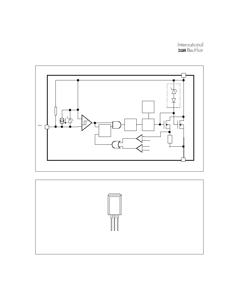
Functional Block Diagram
Lead Assignments
1 2 3
In Vcc Out
2 (Vcc)
Super TO220
4.1V
4.7V
+
-
6mA
+
-
+
-
S
R
Q
Level
shift
driver
Charge
pump
100A
Tj
165∞C
clamp
VCC
IN
35V
40V
Over
temperatur
Over
curren
VOUT
10k

IPS5551T
www.irf.com
5
Figure 3 - Switching time definitions (turn-off)
Figure 4 - Protection timing diagram
90%
10 %
Td off
Tf
Vcc-Vout
Vcc-Vin
DV/dt(off)
Figure 2 - Switching time definitions (turn-on)
Figure 1 - Voltages and currents definition
IPS 5551
Vcc-Vin
Vcc-Vin
max
Vcc-Vin1
max
Vcc-Vin (op)
Vih
Vil
Vhys
Iin
Iin
max
Iin1,2
Iin(on)
Vcc-Vout
Vcc-Vout
max
Vclamp1
Vclamp2
Iout
Iout
max
-Ids
cont.
-Ids
pulsed
Iout
85∞C
Isd
Iq
Vcc
In
Out
Vcc
10 %
Td on
Tr1
Vcc-Vout
Vcc-Vin
90%
Tr2
DV/dt(on)
5V
Tjsd
Iout
Isd
OI shutdown
Tj
OT shutdown
t < T reset
t > T reset
12V
0 V
Vcc-Vin