Äîêóìåíòàöèÿ è îïèñàíèÿ www.docs.chipfind.ru
Typical Connection
HIGH AND LOW SIDE DRIVER
Features
·
Floating channel designed for bootstrap operation
Fully operational to +600V
Tolerant to negative transient voltage
dV/dt immune
·
Gate drive supply range from 10 to 20V (IR2106(4))
·
Undervoltage lockout for both channels
·
3.3V, 5V and 15V input logic compatible
·
Matched propagation delay for both channels
·
Logic and power ground +/- 5V offset.
·
Lower di/dt gate driver for better noise immunity
·
Outputs in phase with inputs (IR2106)
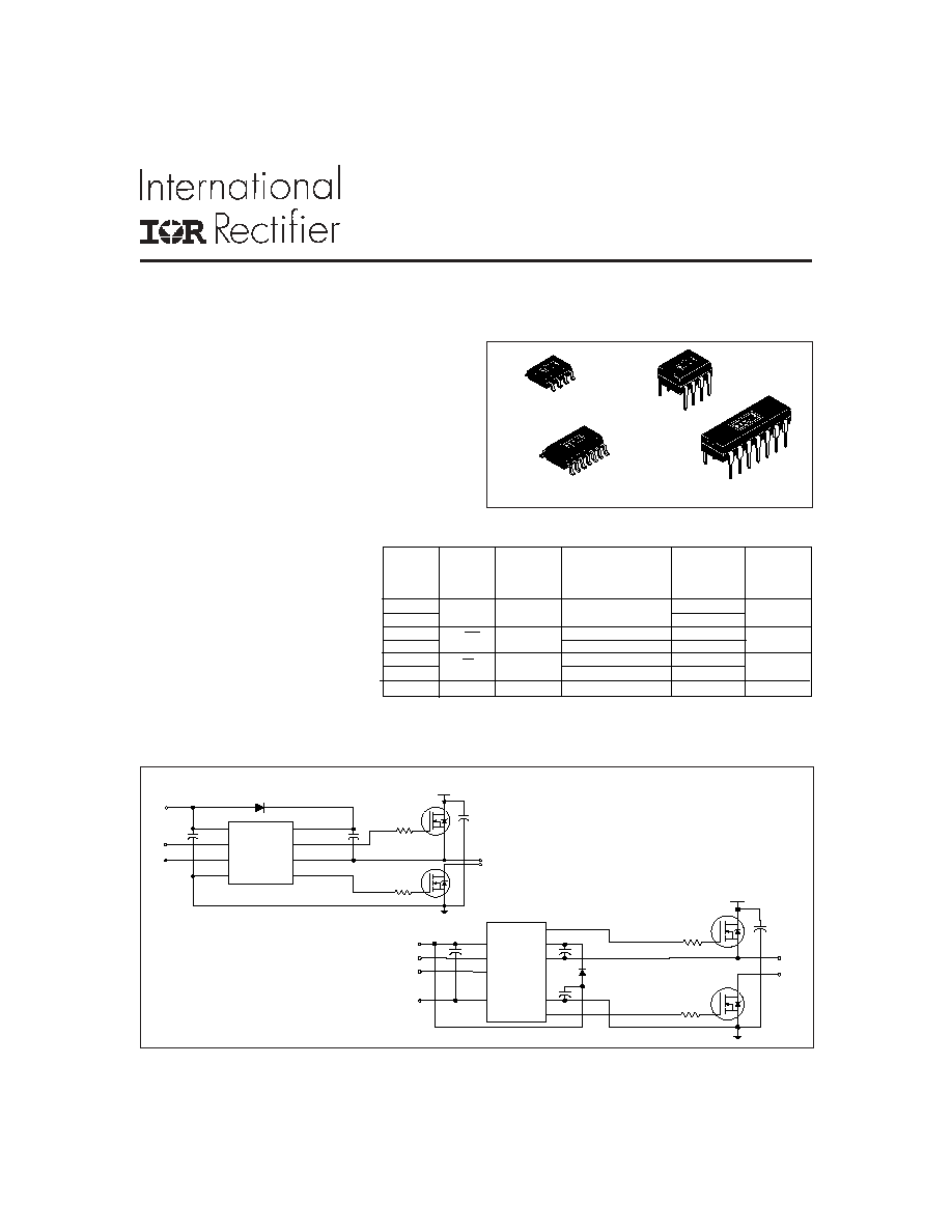
Packages
14-Lead PDIP
14-Lead SOIC
IR2106(4)
(S)
8-Lead PDIP
8-Lead SOIC
www.irf.com
1
Data Sheet No. PD60162 Rev. V
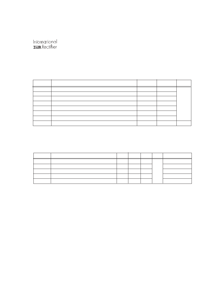
(Refer to Lead Assignments for cor-
rect pin configuration). This/These
diagram(s) show electrical connec-
tions only. Please refer to our Appli-
cation Notes and DesignTips for
proper circuit board layout.
Part
Input
logic
Cross-
conduction
prevention
logic
Dead-Time
Ground Pins
Ton/Toff
2106/2301
COM
21064
HIN/LIN
no
none
VSS/COM
220/200
2108
Internal 540ns
COM
21084
HIN/LIN
yes
Programmable 0.54~5
µ
s
VSS/COM
220/200
2109/2302
Internal 540ns
COM
21094
IN/SD
yes
Programmable 0.54~5
µ
s
VSS/COM
750/200
2106/2301//2108//2109/2302/2304
Feature Comparison
2304
HIN/LIN
yes
Internal 100ns
COM
160/140
Description
The IR2106(4)(S) are high voltage,
high speed power MOSFET and
IGBT drivers with independent high
and low side referenced output chan-
nels. Proprietary HVIC and latch
immune CMOS technologies enable
ruggedized monolithic construction.
The logic input is compatible with
standard CMOS or LSTTL output,
down to 3.3V logic. The output driv-
ers feature a high pulse current buffer stage designed for minimum driver cross-conduction. The floating
channel can be used to drive an N-channel power MOSFET or IGBT in the high side configuration which
operates up to 600 volts.
IR2106
V
CC
V
B
V
S
HO
LO
COM
HIN
LIN
up to 600V
TO
LOAD
V
CC
LIN
HIN
IR21064
up to 600V
TO
LOAD
V
CC
V
B
V
S
HO
LO
COM
HIN
V
SS
LIN
V
CC
V
SS
LIN
HIN
IR2106(4)
(S)
2
www.irf.com
Symbol
Definition
Min.
Max.
Units
V
B
High side floating absolute voltage
-0.3
625
V
S
High side floating supply offset voltage
V
B
- 25
V
B
+ 0.3
V
HO
High side floating output voltage
V
S
- 0.3
V
B
+ 0.3
V
CC
Low side and logic fixed supply voltage
-0.3
25
V
LO
Low side output voltage
-0.3
V
CC
+ 0.3
V
IN
Logic input voltage
V
SS
- 0.3 V
CC
+ 0.3
V
SS
Logic ground (IR21064 only)
V
CC
- 25
V
CC
+ 0.3
dV
S
/dt
Allowable offset supply voltage transient
--
50
V/ns
P
D
Package power dissipation @ T
A
+25
°
C
(8 lead PDIP)
--
1.0
(8 lead SOIC)
--
0.625
(14 lead PDIP)
--
1.6
(14 lead SOIC)
--
1.0
Rth
JA
Thermal resistance, junction to ambient
(8 lead PDIP)
--
125
(8 lead SOIC)
--
200
(14 lead PDIP)
--
75
(14 lead SOIC)
--
120
T
J
Junction temperature
--
150
T
S
Storage temperature
-50
150
T
L
Lead temperature (soldering, 10 seconds)
--
300
Absolute Maximum Ratings
Absolute maximum ratings indicate sustained limits beyond which damage to the device may occur. All voltage param-
eters are absolute voltages referenced to COM. The thermal resistance and power dissipation ratings are measured
under board mounted and still air conditions.
V
°
C
°
C/W
W
IR2106(4)
(S)
www.irf.com
3
Dynamic Electrical Characteristics
V
BIAS
(V
CC
, V
BS
) = 15V, V
SS
= COM, C
L
= 1000 pF, T
A
= 25
°
C.
Symbol
Definition
Min. Typ.
Max. Units Test Conditions
ton
Turn-on propagation delay
--
220
300
V
S
= 0V
toff
Turn-off propagation delay
--
200
280
V
S
= 0V or 600V
MT
Delay matching, HS & LS turn-on/off
--
0
30
tr
Turn-on rise time
--
150
220
V
S
= 0V
tf
Turn-off fall time
--
50
80
V
S
= 0V
nsec
Note 1: Logic operational for V
S
of -5 to +600V. Logic state held for V
S
of -5V to -V
BS
. (Please refer to the Design Tip
DT97-3 for more details).
VB
High side floating supply absolute voltage IR2106(4)
V
S
+ 10
V
S
+ 20
V
S
High side floating supply offset voltage
Note 1
600
V
HO
High side floating output voltage
V
S
V
B
V
CC
Low side and logic fixed supply voltage IR2106(4)
10
20
V
LO
Low side output voltage
0
V
CC
V
IN
Logic input voltage
V
SS
V
CC
V
SS
Logic ground (IR21064 only)
-5
5
T
A
Ambient temperature
-40
125
°C
V
Symbol
Definition
Min.
Max.
Units
Recommended Operating Conditions
The Input/Output logic timing diagram is shown in figure 1. For proper operation the device should be used within the
recommended conditions. The V
S
and V
SS
offset rating are tested with all supplies biased at 15V differential.
IR2106(4)
(S)
4
www.irf.com
Static Electrical Characteristics
V
BIAS
(V
CC
, V
BS
) = 15V, V
SS
= COM and T
A
= 25
°
C unless otherwise specified. The V
IL
, V
IH
and I
IN
parameters are
referenced to V
SS
/COM and are applicable to the respective input leads. The V
O
, I
O
and Ron parameters are referenced to
COM and are applicable to the respective output leads: HO and LO.
Symbol
Definition
Min. Typ. Max. Units Test Conditions
V
IH
Logic "1" input voltage (IR2106(4))
2.9 -- --
V
CC
= 10V to 20V
V
IL
Logic "0" input voltage (IR2106(4))
-- -- 0.8
V
CC
= 10V to 20V
V
OH
High level output voltage, V
BIAS
- V
O
--
0.8
1.4
I
O
= 20 mA
V
OL
Low level output voltage, V
O
--
0.3
0.6
I
O
= 20 mA
I
LK
Offset supply leakage current
--
--
50
V
B
= V
S
= 600V
I
QBS
Quiescent V
BS
supply current
20
75
130
V
IN
= 0V or 5V
I
QCC
Quiescent V
CC
supply current
60
120
180
V
IN
= 0V or 5V
I
IN+
Logic "1" input bias current
V
IN
= 5V (IR2106(4))
-- 5 20
I
IN-
Logic "0" input bias current
V
IN
= 0V (IR2106(4))
-- -- 2
V
CCUV+
V
CC
and V
BS
supply undervoltage positive going
8.0
8.9
9.8
V
BSUV+
threshold
V
CCUV-
V
CC
and V
BS
supply undervoltage negative going
7.4
8.2
9.0
V
BSUV-
threshold
V
CCUVH
Hysteresis
0.3
0.7
--
V
BSUVH
I
O+
Output high short circuit pulsed current
120
200
--
V
O
= 0V,
PW
10
µ
s
I
O-
Output low short circuit pulsed current
250
350
--
V
O
= 15V,
PW
10
µ
s
V
µ
A
mA
V
IR2106(4)
(S)
www.irf.com
5
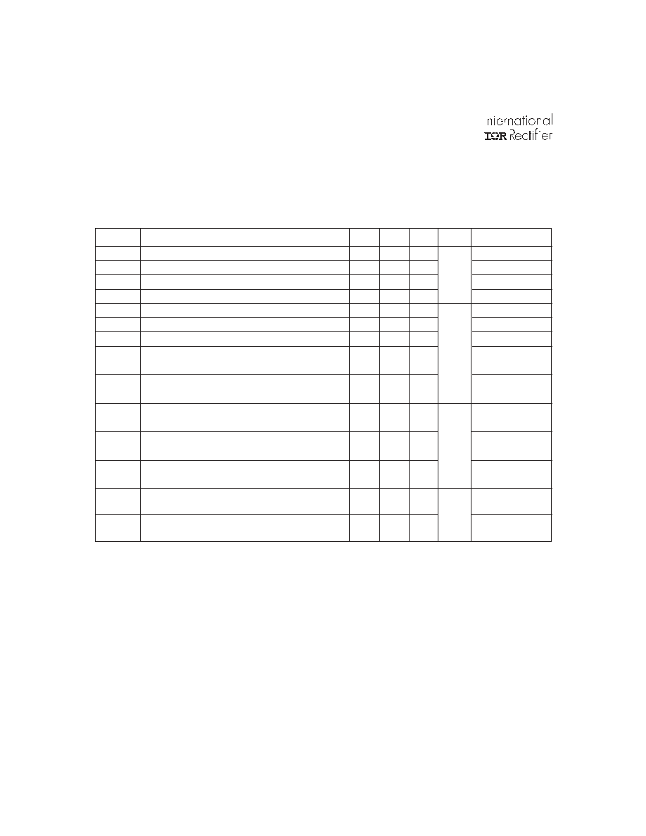
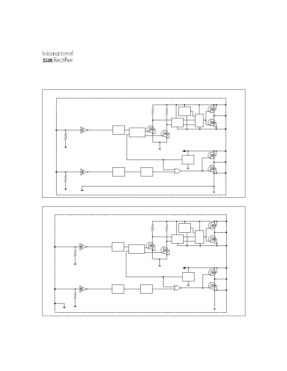
Functional Block Diagrams
IR2106
LIN
UV
DETECT
DELAY
COM
LO
VCC
HIN
VS
HO
VB
PULSE
FILTER
HV
LEVEL
SHIFTER
R
R
S
Q
UV
DETECT
PULSE
GENERATOR
VSS/COM
LEVEL
SHIFT
VSS/COM
LEVEL
SHIFT
IR21064
LIN
UV
DETECT
DELAY
COM
LO
VCC
HIN
VSS
VS
HO
VB
PULSE
FILTER
HV
LEVEL
SHIFTER
R
R
S
Q
UV
DETECT
PULSE
GENERATOR
VSS/COM
LEVEL
SHIFT
VSS/COM
LEVEL
SHIFT