Äîêóìåíòàöèÿ è îïèñàíèÿ www.docs.chipfind.ru
06/29/04
www.irf.com
1
HEXFET
®
is a registered trademark of International Rectifier.
IRF1010EZPbF
IRF1010EZSPbF
IRF1010EZLPbF
HEXFET
®
Power MOSFET
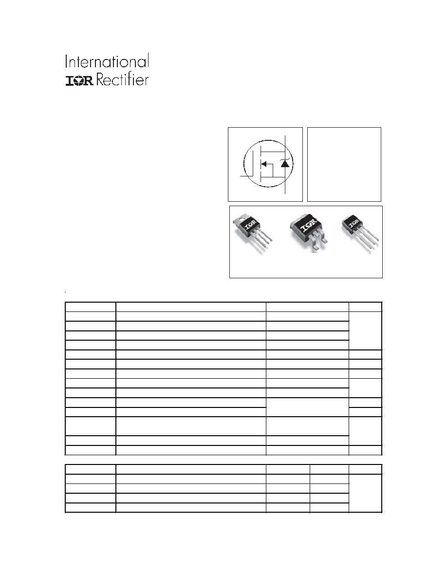
S
D
G
V
DSS
= 60V
R
DS(on)
= 8.5m
I
D
= 75A
Features
Advanced Process Technology
Ultra Low On-Resistance
Dynamic dv/dt Rating
175°C Operating Temperature
Fast Switching
Repetitive Avalanche Allowed up to Tjmax
AUTOMOTIVE MOSFET
Description
Specifically designed for Automotive applications,
this HEXFET
®
Power MOSFET utilizes the latest
processing techniques to achieve extremely low
on-resistance per silicon area. Additional fea-
tures of this design are a 175°C junction operat-
ing temperature, fast switching speed and im-
proved repetitive avalanche rating . These fea-
tures combine to make this design an extremely
efficient and reliable device for use in Automotive
applications and a wide variety of other applica-
tions.
D
2
Pak
IRF1010EZS
TO-220AB
IRF1010EZ
TO-262
IRF1010EZL
Absolute Maximum Ratings
Parameter
Units
I
D
@ T
C
= 25°C
Continuous Drain Current, V
GS
@ 10V (Silicon Limited)
A
I
D
@ T
C
= 100°C
Continuous Drain Current, V
GS
@ 10V (See Fig. 9)
I
D
@ T
C
= 25°C
Continuous Drain Current, V
GS
@ 10V
(Package Limited)
I
DM
Pulsed Drain Current
c
P
D
@T
C
= 25°C
Maximum Power Dissipation
W
Linear Derating Factor
W/°C
V
GS
Gate-to-Source Voltage
V
E
AS
Single Pulse Avalanche Energy (Thermally Limited)
d
mJ
E
AS
(tested)
Single Pulse Avalanche Energy Tested Value
i
I
AR
Avalanche Current
c
A
E
AR
Repetitive Avalanche Energy
h
mJ
T
J
Operating Junction and
°C
T
STG
Storage Temperature Range
Soldering Temperature, for 10 seconds
Mounting torque, 6-32 or M3 screw
Thermal Resistance
Parameter
Typ.
Max.
Units
R
JC
Junction-to-Case
1.11
°C/W
R
CS
Case-to-Sink, Flat, Greased Surface
0.50
R
JA
Junction-to-Ambient
62
R
JA
Junction-to-Ambient (PCB Mount, steady state)
j
40
Max.
84
60
340
75
10 lbf·in (1.1N·m)
140
0.90
± 20
99
180
See Fig.12a,12b,15,16
300 (1.6mm from case )
-55 to + 175
PD - 95483
Lead-Free
IRF1010EZ/S/LPbF
2
www.irf.com
Notes:
Repetitive rating; pulse width limited by
max. junction temperature. (See fig. 11).
Limited by T
Jmax
, starting T
J
= 25°C, L = 0.077mH,
R
G
= 25
, I
AS
= 51A, V
GS
=10V. Part not
recommended for use above this value.
I
SD
51A, di/dt
260A/µs, V
DD
V
(BR)DSS
,
T
J
175°C.
Pulse width
1.0ms; duty cycle
2%.
C
oss
eff. is a fixed capacitance that gives the same charging time
as C
oss
while V
DS
is rising from 0 to 80% V
DSS
.
Limited by T
Jmax
, see Fig.12a, 12b, 15, 16 for typical repetitive
avalanche performance.
This value determined from sample failure population. 100%
tested to this value in production.
This is applied to D
2
Pak, when mounted on 1" square PCB
( FR-4 or G-10 Material ). For recommended footprint and
soldering techniques refer to application note #AN-994.
S
D
G
S
D
G
Static @ T
J
= 25°C (unless otherwise specified)
Parameter
Min. Typ. Max. Units
V
(BR)DSS
Drain-to-Source Breakdown Voltage
60
V
V
DSS
/
T
J
Breakdown Voltage Temp. Coefficient
0.058
V/°C
R
DS(on)
Static Drain-to-Source On-Resistance
6.8
8.5
m
V
GS(th)
Gate Threshold Voltage
2.0
4.0
V
gfs
Forward Transconductance
200
S
I
DSS
Drain-to-Source Leakage Current
20
µA
250
I
GSS
Gate-to-Source Forward Leakage
200
nA
Gate-to-Source Reverse Leakage
-200
Q
g
Total Gate Charge
58
86
nC
Q
gs
Gate-to-Source Charge
19
28
Q
gd
Gate-to-Drain ("Miller") Charge
21
32
t
d(on)
Turn-On Delay Time
19
ns
t
r
Rise Time
90
t
d(off)
Turn-Off Delay Time
38
t
f
Fall Time
54
L
D
Internal Drain Inductance
4.5
nH
Between lead,
6mm (0.25in.)
L
S
Internal Source Inductance
7.5
from package
and center of die contact
C
iss
Input Capacitance
2810
pF
C
oss
Output Capacitance
420
C
rss
Reverse Transfer Capacitance
200
C
oss
Output Capacitance
1440
C
oss
Output Capacitance
320
C
oss
eff.
Effective Output Capacitance
510
Diode Characteristics
Parameter
Min. Typ. Max. Units
I
S
Continuous Source Current
84
(Body Diode)
A
I
SM
Pulsed Source Current
340
(Body Diode)
Ã
V
SD
Diode Forward Voltage
1.3
V
t
rr
Reverse Recovery Time
41
62
ns
Q
rr
Reverse Recovery Charge
54
81
nC
t
on
Forward Turn-On Time
Intrinsic turn-on time is negligible (turn-on is dominated by LS+LD)
Conditions
V
GS
= 0V, I
D
= 250µA
Reference to 25°C, I
D
= 1mA
V
GS
= 10V, I
D
= 51A
f
V
DS
= V
GS
, I
D
= 250µA
V
DS
= 60V, V
GS
= 0V
V
DS
= 60V, V
GS
= 0V, T
J
= 125°C
R
G
= 7.95
I
D
= 51A
V
DS
= 25V, I
D
= 51A
V
DD
= 30V
I
D
= 51A
V
GS
= 20V
V
GS
= -20V
T
J
= 25°C, I
F
= 51A, V
DD
= 30V
di/dt = 100A/µs
f
T
J
= 25°C, I
S
= 51A, V
GS
= 0V
f
showing the
integral reverse
p-n junction diode.
MOSFET symbol
V
GS
= 0V
V
DS
= 25V
V
GS
= 0V, V
DS
= 48V, = 1.0MHz
Conditions
V
GS
= 0V, V
DS
= 0V to 48V
V
DS
= 48V
V
GS
= 10V
f
= 1.0MHz, See Fig. 5
V
GS
= 0V, V
DS
= 1.0V, = 1.0MHz
V
GS
= 10V
f
IRF1010EZ/S/LPbF
www.irf.com
3
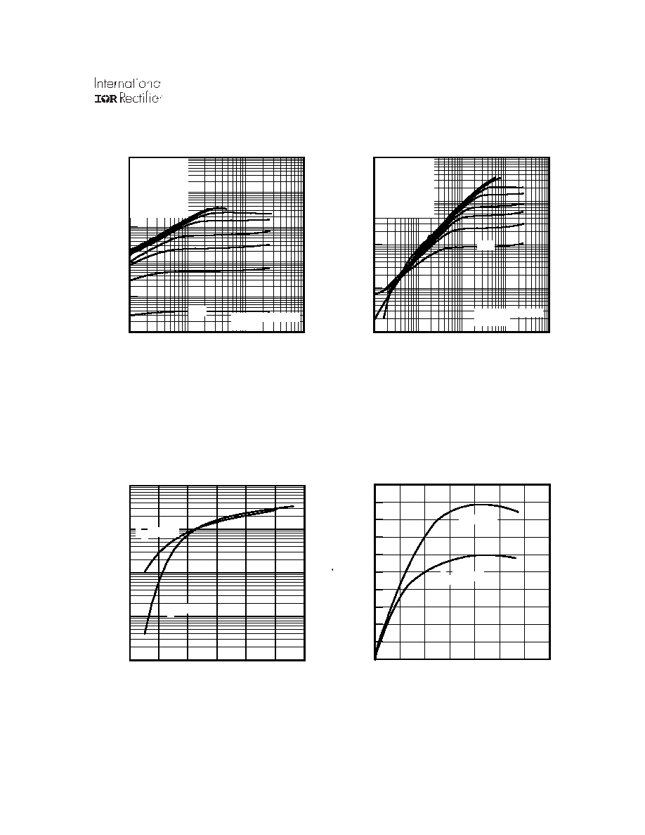
Fig 2. Typical Output Characteristics
Fig 1. Typical Output Characteristics
Fig 3. Typical Transfer Characteristics
Fig 4. Typical Forward Transconductance
vs. Drain Current
0.01
0.1
1
10
100
VDS, Drain-to-Source Voltage (V)
0.1
1
10
100
1000
I D
,
D
r
a
i
n
-
t
o
-
S
o
u
r
c
e
C
u
r
r
e
n
t
(
A
)
20µs PULSE WIDTH
Tj = 175°C
4.5V
VGS
TOP
15V
10V
8.0V
7.0V
6.0V
5.5V
5.0V
BOTTOM
4.5V
4
5
6
7
8
9
10
VGS, Gate-to-Source Voltage (V)
0.1
1
10
100
1000
I D
,
D
r
a
i
n
-
t
o
-
S
o
u
r
c
e
C
u
r
r
e
n
t
(
)
TJ = 25°C
TJ = 175°C
0.1
1
10
100
VDS, Drain-to-Source Voltage (V)
0.1
1
10
100
1000
10000
I D
,
D
r
a
i
n
-
t
o
-
S
o
u
r
c
e
C
u
r
r
e
n
t
(
A
)
VGS
TOP
15V
10V
8.0V
7.0V
6.0V
5.5V
5.0V
BOTTOM
4.5V
20µs PULSE WIDTH
Tj = 25°C
4.5V
0
20
40
60
80
100
120
140
ID,Drain-to-Source Current (A)
0
10
20
30
40
50
60
70
80
90
100
G
f
s
,
F
o
r
w
a
r
d
T
r
a
n
s
c
o
n
d
u
c
t
a
n
c
e
(
S
)
TJ = 25°C
TJ = 175°C
IRF1010EZ/S/LPbF
4
www.irf.com
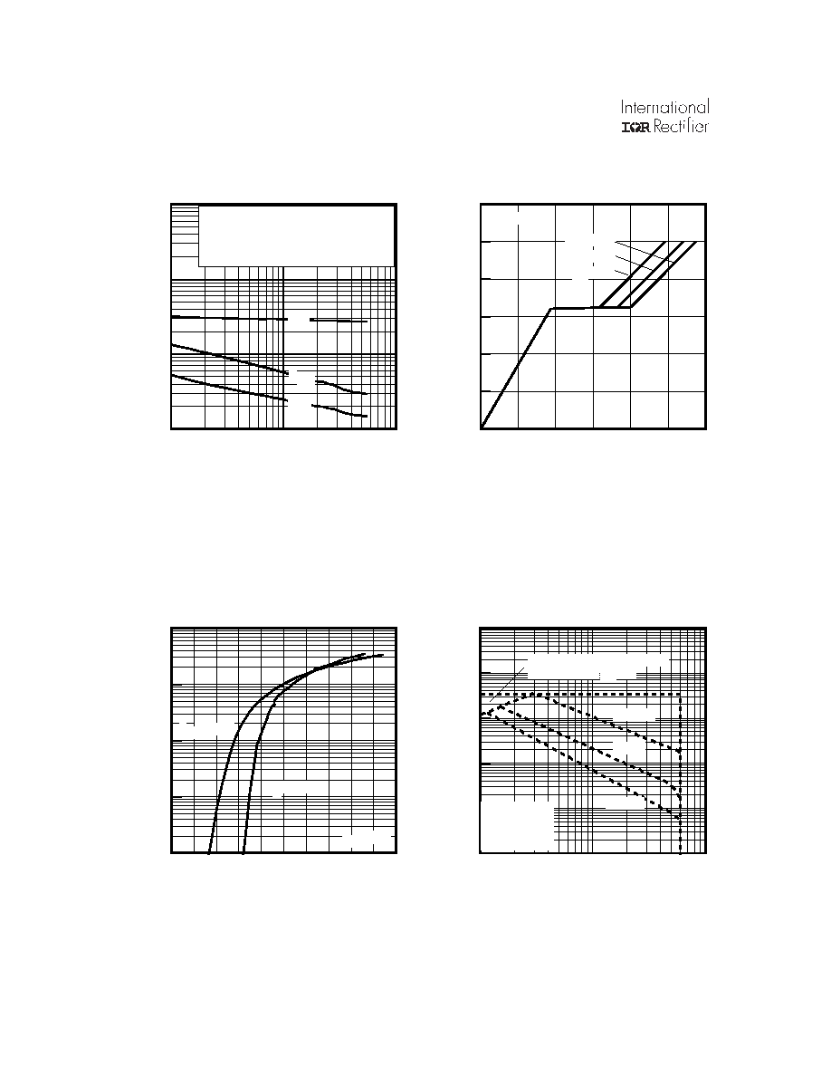
Fig 8. Maximum Safe Operating Area
Fig 6. Typical Gate Charge vs.
Gate-to-Source Voltage
Fig 5. Typical Capacitance vs.
Drain-to-Source Voltage
Fig 7. Typical Source-Drain Diode
Forward Voltage
1
10
100
VDS, Drain-to-Source Voltage (V)
100
1000
10000
100000
C
,
C
a
p
a
c
i
t
a
n
c
e
(
p
F
)
VGS = 0V, f = 1 MHZ
Ciss = C gs + Cgd, C ds SHORTED
Crss = Cgd
Coss = Cds + Cgd
Coss
Crss
Ciss
0
10
20
30
40
50
60
QG Total Gate Charge (nC)
0.0
2.0
4.0
6.0
8.0
10.0
12.0
V
G
S
,
G
a
t
e
-
t
o
-
S
o
u
r
c
e
V
o
l
t
a
g
e
(
V
)
VDS= 48V
VDS= 30V
VDS= 12V
ID= 51A
0.0 0.2 0.4 0.6 0.8 1.0 1.2 1.4 1.6 1.8 2.0
VSD, Source-to-Drain Voltage (V)
0.10
1.00
10.00
100.00
1000.00
I S
D
,
R
e
v
e
r
s
e
D
r
a
i
n
C
u
r
r
e
n
t
(
A
)
TJ = 25°C
TJ = 175°C
VGS = 0V
1
10
100
VDS, Drain-to-Source Voltage (V)
0.1
1
10
100
1000
10000
I D
,
D
r
a
i
n
-
t
o
-
S
o
u
r
c
e
C
u
r
r
e
n
t
(
A
)
1msec
10msec
OPERATION IN THIS AREA
LIMITED BY R DS(on)
100µsec
Tc = 25°C
Tj = 175°C
Single Pulse
IRF1010EZ/S/LPbF
www.irf.com
5
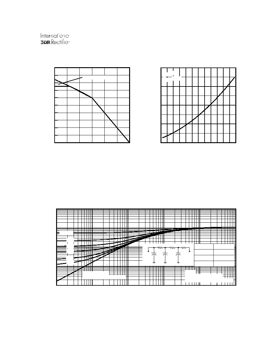
Fig 11. Maximum Effective Transient Thermal Impedance, Junction-to-Case
Fig 9. Maximum Drain Current vs.
Case Temperature
Fig 10. Normalized On-Resistance
vs. Temperature
-60 -40 -20
0
20 40 60 80 100 120 140 160 180
TJ , Junction Temperature (°C)
0.5
1.0
1.5
2.0
2.5
R
D
S
(
o
n
)
,
D
r
a
i
n
-
t
o
-
S
o
u
r
c
e
O
n
R
e
s
i
s
t
a
n
c
e
(
N
o
r
m
a
l
i
z
e
d
)
ID = 84A
VGS = 10V
1E-006
1E-005
0.0001
0.001
0.01
0.1
t1 , Rectangular Pulse Duration (sec)
0.001
0.01
0.1
1
10
T
h
e
r
m
a
l
R
e
s
p
o
n
s
e
(
Z
t
h
J
C
)
0.20
0.10
D = 0.50
0.02
0.01
0.05
SINGLE PULSE
( THERMAL RESPONSE )
Notes:
1. Duty Factor D = t1/t2
2. Peak Tj = P dm x Zthjc + Tc
Ri (°C/W)
i (sec)
0.415 0.000246
0.410 0.000898
0.285 0.009546
J
J
1
1
2
2
3
3
R
1
R
1
R
2
R
2
R
3
R
3
C
Ci= i
/
Ri
Ci=
i
/
Ri
25
50
75
100
125
150
175
TC , Case Temperature (°C)
0
10
20
30
40
50
60
70
80
90
100
I D
,
D
r
a
i
n
C
u
r
r
e
n
t
(
A
)
Limited By Package