 | ÐлекÑÑоннÑй компоненÑ: IRF1312S | СкаÑаÑÑ:  PDF PDF  ZIP ZIP |
Äîêóìåíòàöèÿ è îïèñàíèÿ www.docs.chipfind.ru
Notes
through
are on page 11
www.irf.com
1
7/01/02
HEXFET
®
Power MOSFET
V
DSS
R
DS(on)
max
I
D
80V
10m
95A
PD- 94504
Absolute Maximum Ratings
l
High frequency DC-DC converters
l
Motor Control
l
Uninterrutible Power Supplies
Benefits
Applications
l
Low Gate-to-Drain Charge to Reduce
Switching Losses
l
Fully Characterized Capacitance Including
Effective C
OSS
to Simplify Design, (See
App. Note AN1001)
l
Fully Characterized Avalanche Voltage
and Current
D
2
Pak
IRF1312S
TO-220AB
IRF1312
TO-262
IRF1312L
IRF1312
IRF1312S
IRF1312L
Thermal Resistance
Parameter
Typ.
Max.
Units
R
JC
Junction-to-Case
0.73
R
CS
Case-to-Sink, Flat, Greased Surface
0.50
°C/W
R
JA
Junction-to-Ambient
62
R
JA
Junction-to-Ambient (PCB mount)
40
Parameter
Max.
Units
I
D
@ T
C
= 25°C
Continuous Drain Current, V
GS
@ 10V
95
I
D
@ T
C
= 100°C
Continuous Drain Current, V
GS
@ 10V
67
A
I
DM
Pulsed Drain Current
380
P
D
@T
A
= 25°C
Power Dissipation
3.8
W
P
D
@T
C
= 25°C
Power Dissipation
210
Linear Derating Factor
1.4
W/°C
V
GS
Gate-to-Source Voltage
± 20
V
dv/dt
Peak Diode Recovery dv/dt
5.1
V/ns
T
J
Operating Junction and
-55 to + 175
T
STG
Storage Temperature Range
Soldering Temperature, for 10 seconds
300 (1.6mm from case )
°C
Mounting torqe, 6-32 or M3 screw 10 lbf·in (1.1N·m)
IRF1312/S/L
2
www.irf.com
Parameter
Min. Typ. Max. Units
Conditions
g
fs
Forward Transconductance
92
S
V
DS
= 25V, I
D
= 57A
Q
g
Total Gate Charge
93 140 I
D
= 57A
Q
gs
Gate-to-Source Charge
36
nC
V
DS
= 40V
Q
gd
Gate-to-Drain ("Miller") Charge
34
V
GS
= 10V,
t
d(on)
Turn-On Delay Time
25
V
DD
= 40V
t
r
Rise Time
130
I
D
= 57A
t
d(off)
Turn-Off Delay Time
47
R
G
= 4.5
t
f
Fall Time
51
V
GS
= 10V
C
iss
Input Capacitance
5450
V
GS
= 0V
C
oss
Output Capacitance
550
V
DS
= 25V
C
rss
Reverse Transfer Capacitance
340
pF
= 1.0MHz
C
oss
Output Capacitance
1910
V
GS
= 0V, V
DS
= 1.0V, = 1.0MHz
C
oss
Output Capacitance
380
V
GS
= 0V, V
DS
= 64V, = 1.0MHz
C
oss
eff.
Effective Output Capacitance
620
V
GS
= 0V, V
DS
= 0V to 64V
Dynamic @ T
J
= 25°C (unless otherwise specified)
ns
Parameter
Typ.
Max.
Units
E
AS
Single Pulse Avalanche Energy
250
mJ
I
AR
Avalanche Current
57
A
E
AR
Repetitive Avalanche Energy
21
mJ
Avalanche Characteristics
S
D
G
Parameter
Min. Typ. Max. Units
Conditions
I
S
Continuous Source Current
MOSFET symbol
(Body Diode)
showing the
I
SM
Pulsed Source Current
integral reverse
(Body Diode)
p-n junction diode.
V
SD
Diode Forward Voltage
1.3
V
T
J
= 25°C, I
S
= 57A, V
GS
= 0V
t
rr
Reverse Recovery Time
64
96
ns
T
J
= 25°C, I
F
= 57A
Q
rr
Reverse RecoveryCharge
150
230
nC
di/dt = 100A/µs
t
on
Forward Turn-On Time
Intrinsic turn-on time is negligible (turn-on is dominated by L
S
+L
D
)
Diode Characteristics
95
380
A
Static @ T
J
= 25°C (unless otherwise specified)
Parameter
Min. Typ. Max. Units
Conditions
V
(BR)DSS
Drain-to-Source Breakdown Voltage
80
V
V
GS
= 0V, I
D
= 250µA
V
(BR)DSS
/
T
J
Breakdown Voltage Temp. Coefficient
0.078 V/°C Reference to 25°C, I
D
= 1mA
R
DS(on)
Static Drain-to-Source On-Resistance
6.6
10
m
V
GS
= 10V, I
D
= 57A
V
GS(th)
Gate Threshold Voltage
3.5
5.5
V
V
DS
= V
GS
, I
D
= 250µA
1.0
µA
V
DS
= 76V, V
GS
= 0V
250
V
DS
= 64V, V
GS
= 0V, T
J
= 150°C
Gate-to-Source Forward Leakage
100
V
GS
= 20V
Gate-to-Source Reverse Leakage
-100
nA
V
GS
= -20V
I
GSS
I
DSS
Drain-to-Source Leakage Current
IRF1312/S/L
www.irf.com
3
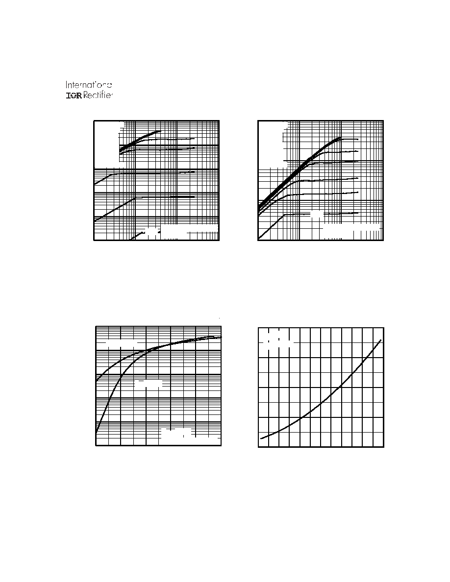
Fig 4. Normalized On-Resistance
Vs. Temperature
Fig 2. Typical Output Characteristics
Fig 1. Typical Output Characteristics
Fig 3. Typical Transfer Characteristics
0.1
1
10
100
VDS, Drain-to-Source Voltage (V)
0.01
0.1
1
10
100
1000
I D
,
D
r
a
i
n
-
t
o
-
S
o
u
r
c
e
C
u
r
r
e
n
t
(
A
)
5.0V
20µs PULSE WIDTH
Tj = 25°C
VGS
TOP 15V
12V
10V
8.0V
7.0V
6.0V
5.5V
BOTTOM 5.0V
0.1
1
10
100
VDS, Drain-to-Source Voltage (V)
1
10
100
1000
I D
,
D
r
a
i
n
-
t
o
-
S
o
u
r
c
e
C
u
r
r
e
n
t
(
A
)
5.0V
20µs PULSE WIDTH
Tj = 25°C
VGS
TOP 15V
12V
10V
8.0V
7.0V
6.0V
5.5V
BOTTOM 5.0V
5
6
7
8
9
10
VGS, Gate-to-Source Voltage (V)
0.01
0.10
1.00
10.00
100.00
1000.00
I D
,
D
r
a
i
n
-
t
o
-
S
o
u
r
c
e
C
u
r
r
e
n
t
(
A
)
TJ = 25°C
TJ = 175°C
VDS = 25V
20µs PULSE WIDTH
-60 -40 -20
0
20 40 60 80 100 120 140 160 180
TJ , Junction Temperature (°C)
0.5
1.0
1.5
2.0
2.5
R
D
S
(
o
n
)
,
D
r
a
i
n
-
t
o
-
S
o
u
r
c
e
O
n
R
e
s
i
s
t
a
n
c
e
(
N
o
r
m
a
l
i
z
e
d
)
ID = 95A
VGS = 10V
IRF1312/S/L
4
www.irf.com
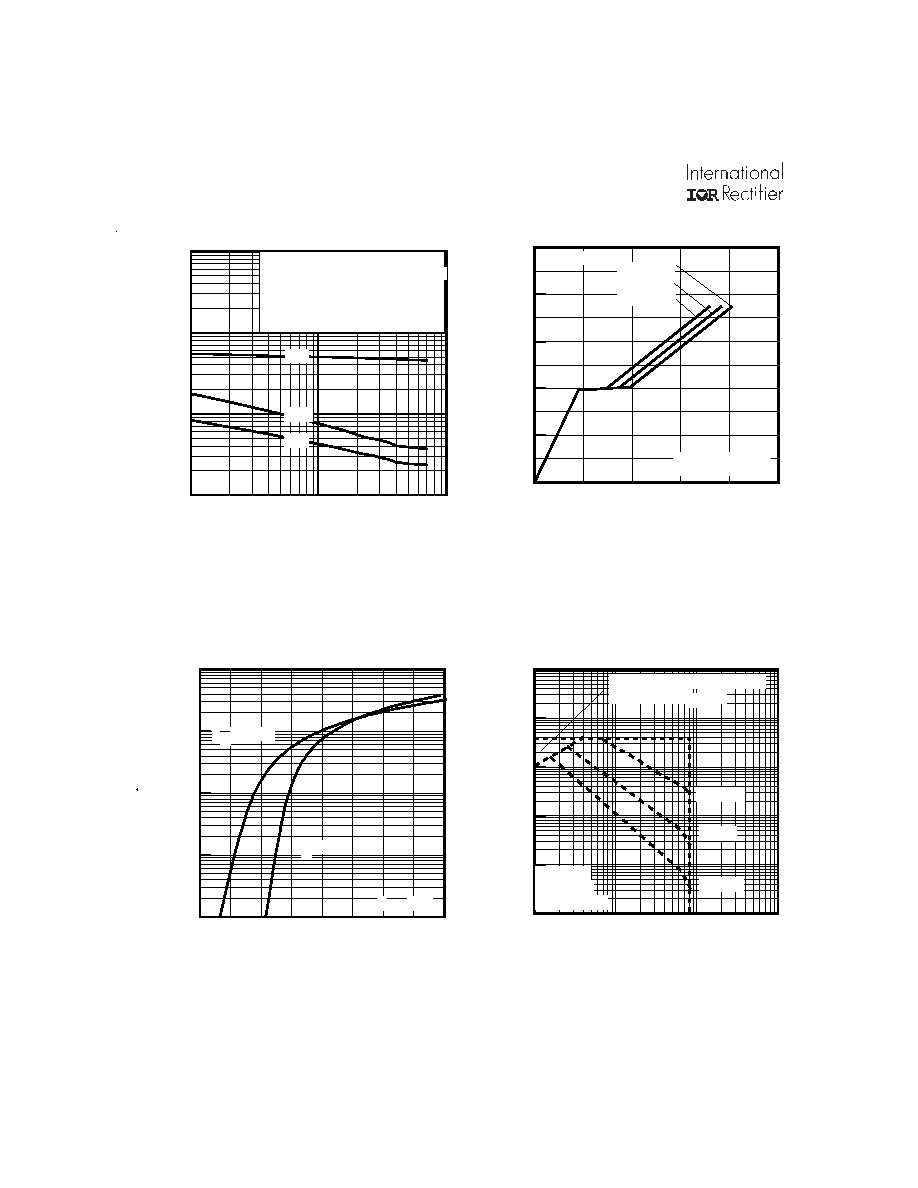
Fig 8. Maximum Safe Operating Area
Fig 6. Typical Gate Charge Vs.
Gate-to-Source Voltage
Fig 5. Typical Capacitance Vs.
Drain-to-Source Voltage
Fig 7. Typical Source-Drain Diode
Forward Voltage
1
10
100
1000
VDS , Drain-toSource Voltage (V)
0.1
1
10
100
1000
10000
I D
,
D
r
a
i
n
-
t
o
-
S
o
u
r
c
e
C
u
r
r
e
n
t
(
A
)
Tc = 25°C
Tj = 175°C
Single Pulse
1msec
10msec
OPERATION IN THIS AREA
LIMITED BY RDS(on)
100µsec
0
40
80
120
160
200
QG Total Gate Charge (nC)
0
4
8
12
16
20
V
G
S
,
G
a
t
e
-
t
o
-
S
o
u
r
c
e
V
o
l
t
a
g
e
(
V
)
VDS= 64V
VDS= 40V
VDS= 16V
ID= 57A
FOR TEST CIRCUIT
SEE FIGURE 13
0.2
0.4
0.6
0.8
1.0
1.2
1.4
1.6
1.8
VSD, Source-toDrain Voltage (V)
0.1
1.0
10.0
100.0
1000.0
I S
D
,
R
e
v
e
r
s
e
D
r
a
i
n
C
u
r
r
e
n
t
(
A
)
TJ = 25°C
TJ = 175°C
VGS = 0V
1
10
100
VDS, Drain-to-Source Voltage (V)
100
1000
10000
100000
C
,
C
a
p
a
c
i
t
a
n
c
e
(
p
F
)
Coss
Crss
Ciss
VGS = 0V, f = 1 MHZ
C iss = Cgs + Cgd , C ds
SHORTED
Crss = Cgd
Coss = Cds + Cgd
IRF1312/S/L
www.irf.com
5
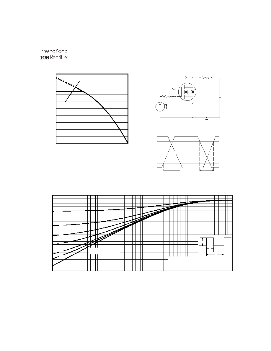
Fig 11. Maximum Effective Transient Thermal Impedance, Junction-to-Case
Fig 9. Maximum Drain Current Vs.
Case Temperature
0.01
0.1
1
0.00001
0.0001
0.001
0.01
0.1
Notes:
1. Duty factor D =
t / t
2. Peak T
= P
x Z
+ T
1
2
J
DM
thJC
C
P
t
t
DM
1
2
t , Rectangular Pulse Duration (sec)
T
her
m
a
l
Res
pons
e
(
Z
)
1
th
JC
0.01
0.02
0.05
0.10
0.20
D = 0.50
SINGLE PULSE
(THERMAL RESPONSE)
V
DS
90%
10%
V
GS
t
d(on)
t
r
t
d(off)
t
f
V
DS
Pulse Width
1
µs
Duty Factor
0.1 %
R
D
V
GS
R
G
D.U.T.
V
GS
+
-
V
DD
Fig 10a. Switching Time Test Circuit
Fig 10b. Switching Time Waveforms
25
50
75
100
125
150
175
TC , Case Temperature (°C)
0
20
40
60
80
100
I D
,
D
r
a
i
n
C
u
r
r
e
n
t
(
A
)
LIMITED BY PACKAGE