/home/web/htmldatasheet/RUSSIAN/html/irf/174432
www.irf.com
1
8/22/00
IRF3707
IRF3707S
SMPS MOSFET
HEXFET
®
Power MOSFET
Benefits
l
Ultra-Low Gate Impedance
l
Very Low R
DS(on)
l
Fully Characterized Avalanche Voltage
and Current
V
DSS
R
DS(on)
max
I
D
30V
12.5m
62A
Notes
through
are on page 10
Absolute Maximum Ratings
Symbol
Parameter
Max.
Units
V
DS
Drain-Source Voltage
30
V
V
GS
Gate-to-Source Voltage
± 20 V
I
D
@ T
C
= 25°C
Continuous Drain Current, V
GS
@ 10V
62
I
D
@ T
C
= 70°C
Continuous Drain Current, V
GS
@ 10V
52
A
I
DM
Pulsed Drain Current
248
P
D
@T
C
= 25°C
Maximum Power Dissipation
87
W
P
D
@T
C
= 70°C
Maximum Power Dissipation
61
W
Linear Derating Factor 0.59 mW/°C
T
J
, T
STG
Junction and Storage Temperature Range
-55 to + 175
°C
* When mounted on 1" square PCB (FR-4 or G-10 Material) .
For recommended footprint and soldering techniques refer to application note #AN-994
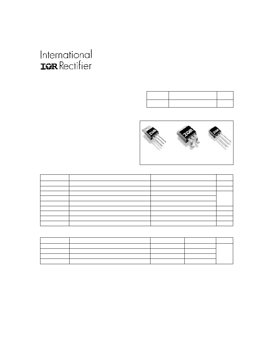
D
2
Pak
IRF3707S
TO-220AB
IRF3707
TO-262
IRF3707L
Thermal Resistance
Parameter
Typ.
Max.
Units
R
JC
Junction-to-Case
1.73
R
CS
Case-to-Sink, Flat, Greased Surface
0.50
°C/W
R
JA
Junction-to-Ambient
62
R
JA
Junction-to-Ambient (PCB mount)*
40
IRF3707L
l
High Frequency DC-DC Isolated
Converters with Synchronous Rectification
for Telecom and Industrial use
Applications
l
High Frequency Buck Converters for
Computer Processor Power
PD - 93937B
IRF3707/3707S/3707L
2
www.irf.com
Dynamic @ T
J
= 25°C (unless otherwise specified)
ns
Symbol
Parameter
Typ.
Max.
Units
E
AS
Single Pulse Avalanche Energy
213
mJ
I
AR
Avalanche Current
62
A
Avalanche Characteristics
S
D
G
Diode Characteristics
62
248
A
Symbol
Parameter
Min. Typ. Max. Units
Conditions
g
fs
Forward Transconductance
37
S
V
DS
= 15V, I
D
= 49.6A
Q
g
Total Gate Charge
19
I
D
= 24.8A
Q
gs
Gate-to-Source Charge
8.2
nC
V
DS
= 15V
Q
gd
Gate-to-Drain ("Miller") Charge
6.3
V
GS
= 4.5V
Q
oss
Output Gate Charge
18
27
V
GS
= 0V, V
DS
= 15V
t
d(on)
Turn-On Delay Time
8.5
V
DD
= 15V
t
r
Rise Time
78
I
D
= 24.8A
t
d(off)
Turn-Off Delay Time
11.8
R
G
= 1.8
t
f
Fall Time
3.3
V
GS
= 4.5V
C
iss
Input Capacitance
1990
V
GS
= 0V
C
oss
Output Capacitance
707
V
DS
= 15V
C
rss
Reverse Transfer Capacitance
50
pF
= 1.0MHz
V
SD
Diode Forward Voltage
Symbol
Parameter
Min. Typ. Max. Units
Conditions
I
S
Continuous Source Current
MOSFET symbol
(Body Diode)
showing the
I
SM
Pulsed Source Current
integral reverse
(Body Diode)
p-n junction diode.
0.88
1.3
V
T
J
= 25°C, I
S
= 31A, V
GS
= 0V
0.8
T
J
= 125°C, I
S
= 31A, V
GS
= 0V
t
rr
Reverse Recovery Time
39
59
ns
T
J
= 25°C, I
F
= 31A, V
R
=20V
Q
rr
Reverse Recovery Charge
49
74
nC
di/dt = 100A/µs
t
rr
Reverse Recovery Time
42
63
ns
T
J
= 125°C, I
F
= 31A, V
R
=20V
Q
rr
Reverse Recovery Charge
62
93
nC
di/dt = 100A/µs
Parameter
Min. Typ. Max. Units
Conditions
V
(BR)DSS
Drain-to-Source Breakdown Voltage
30
V
V
GS
= 0V, I
D
= 250µA
V
(BR)DSS
/
T
J
Breakdown Voltage Temp. Coefficient
0.027 V/°C Reference to 25°C, I
D
= 1mA
9.0
12.5
V
GS
= 10V, I
D
= 15A
12.6
17
V
GS
= 4.5V, I
D
= 12A
V
GS(th)
Gate Threshold Voltage
1.0
3.0
V
V
DS
= V
GS
, I
D
= 250µA
20
µA
V
DS
= 24V, V
GS
= 0V
100
V
DS
= 24V, V
GS
= 0V, T
J
= 125°C
Gate-to-Source Forward Leakage
200
V
GS
= 16V
Gate-to-Source Reverse Leakage
-200
nA
V
GS
= -16V
Static @ T
J
= 25°C (unless otherwise specified)
I
GSS
I
DSS
Drain-to-Source Leakage Current
R
DS(on)
Static Drain-to-Source On-Resistance
m
IRF3707/3707S/3707L
www.irf.com
3
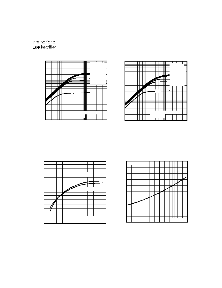
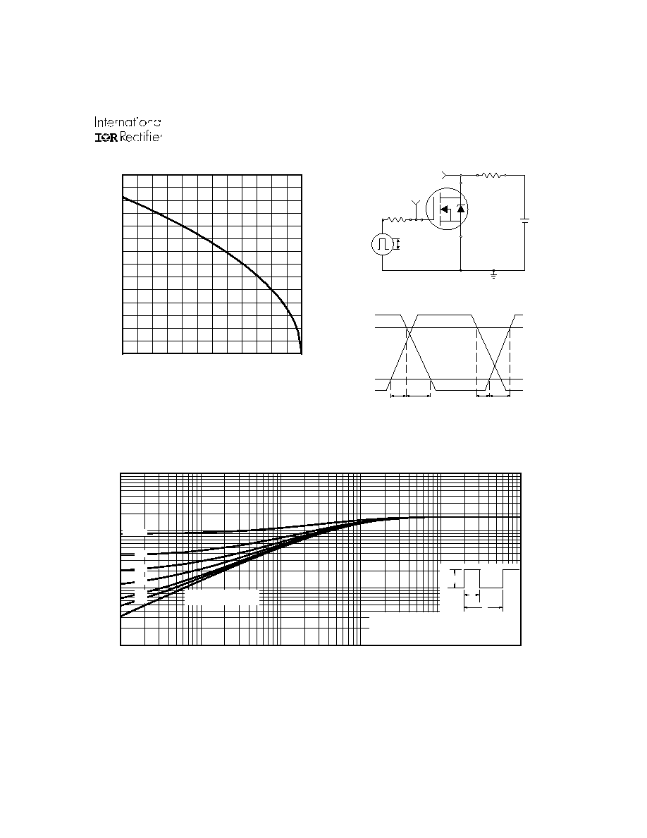
Fig 2. Typical Output Characteristics
Fig 1. Typical Output Characteristics
Fig 3. Typical Transfer Characteristics
Fig 4. Normalized On-Resistance
Vs. Temperature
10
100
1000
3.0
4.0
5.0
6.0
7.0
8.0
V = 15V
20µs PULSE WIDTH
DS
V , Gate-to-Source Voltage (V)
I , Drain-to-Source Current (A)
GS
D
T = 25 C
J
°
T = 175 C
J
°
-60 -40 -20
0
20 40 60
80 100 120 140 160 180
0.0
0.5
1.0
1.5
2.0
2.5
T , Junction Temperature ( C)
R , Drain-to-Source On Resistance
(Normalized)
J
DS(on)
°
V
=
I =
GS
D
10V
62A
0.1
1
10
100
VDS, Drain-to-Source Voltage (V)
1
10
100
1000
I D
, Drain-to-Source Current (A)
3.5V
20µs PULSE WIDTH
Tj = 25°C
VGS
TOP 10.0V
9.0V
8.0V
7.0V
6.0V
5.0V
4.5V
BOTTOM 3.5V
0.1
1
10
100
VDS, Drain-to-Source Voltage (V)
1
10
100
1000
I D
, Drain-to-Source Current (A)
3.5V
20µs PULSE WIDTH
Tj = 175°C
VGS
TOP 10.0V
9.0V
8.0V
7.0V
6.0V
5.0V
4.5V
BOTTOM 3.5V
IRF3707/3707S/3707L
4
www.irf.com
Fig 6. Typical Gate Charge Vs.
Gate-to-Source Voltage
Fig 5. Typical Capacitance Vs.
Drain-to-Source Voltage
Fig 7. Typical Source-Drain Diode
Forward Voltage
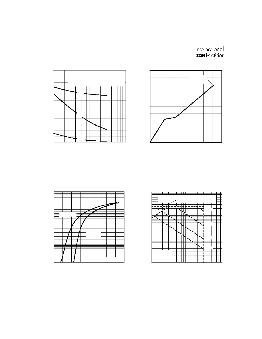
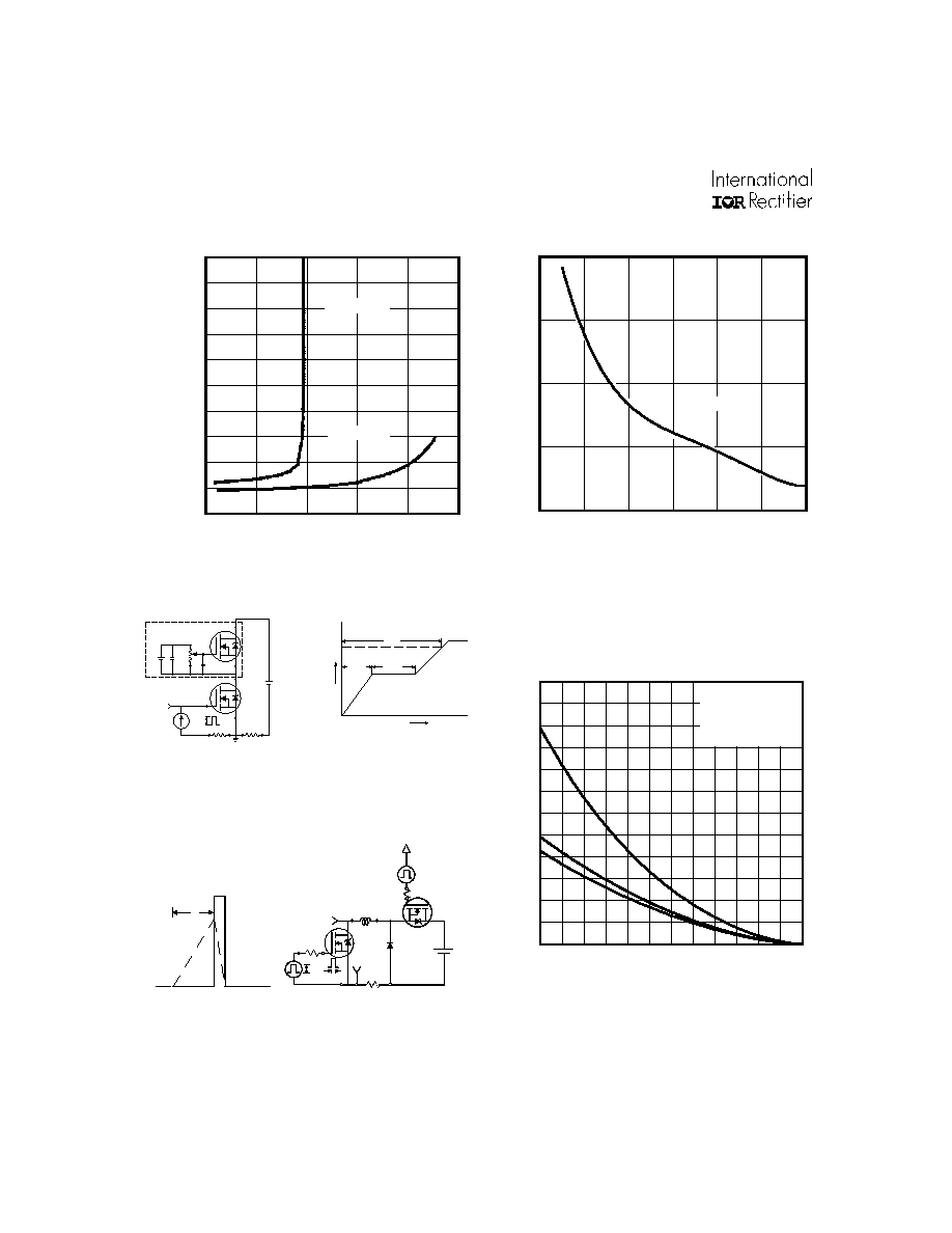
Fig 8. Maximum Safe Operating Area
1
10
100
0
500
1000
1500
2000
2500
3000
V , Drain-to-Source Voltage (V)
C, Capacitance (pF)
DS
V
C
C
C
=
=
=
=
0V,
C
C
C
f = 1MHz
+ C
+ C
C SHORTED
GS
iss
gs
gd ,
ds
rss
gd
oss
ds
gd
Crss
Coss
Ciss
0
10
20
30
40
0
2
4
6
8
10
Q , Total Gate Charge (nC)
V , Gate-to-Source Voltage (V)
G
GS
I =
D
24.8A
V
= 15V
DS
0.1
1
10
100
1000
0.2
0.6
1.0
1.4
1.8
V ,Source-to-Drain Voltage (V)
I , Reverse Drain Current (A)
SD
SD
V = 0 V
GS
T = 25 C
J
°
T = 175 C
J
°
1
10
100
1000
1
10
100
OPERATION IN THIS AREA LIMITED
BY R
DS(on)
Single Pulse
T
T
= 175 C
= 25 C
°
°
J
C
V , Drain-to-Source Voltage (V)
I , Drain Current (A)
I , Drain Current (A)
DS
D
10us
100us
1ms
10ms
IRF3707/3707S/3707L
www.irf.com
5
Fig 11. Maximum Effective Transient Thermal Impedance, Junction-to-Ambient
Fig 9. Maximum Drain Current Vs.
Case Temperature
Fig 10a. Switching Time Test Circuit
V
DS
90%
10%
V
GS
t
d(on)
t
r
t
d(off)
t
f
Fig 10b. Switching Time Waveforms
V
DS
Pulse Width
1
µs
Duty Factor
0.1 %
R
D
V
GS
R
G
D.U.T.
10V
+
-
V
DD
25
50
75
100
125
150
175
0
10
20
30
40
50
60
70
T , Case Temperature ( C)
I , Drain Current (A)
°
C
D
0.01
0.1
1
10
0.00001
0.0001
0.001
0.01
0.1
1
Notes:
1. Duty factor D = t / t
2. Peak T = P
x Z
+ T
1
2
J
DM
thJC
C
P
t
t
DM
1
2
t , Rectangular Pulse Duration (sec)
Thermal Response
(Z )
1
thJC
0.01
0.02
0.05
0.10
0.20
D = 0.50
SINGLE PULSE
(THERMAL RESPONSE)
IRF3707/3707S/3707L
6
www.irf.com
Fig 13. On-Resistance Vs. Gate Voltage
Fig 12. On-Resistance Vs. Drain Current
Fig 15a&b. Unclamped Inductive Test circuit
and Waveforms
Fig 15c. Maximum Avalanche Energy
Vs. Drain Current
D.U.T.
V
DS
I
D
I
G
3mA
V
GS
.3
µ
F
50K
.2
µ
F
12V
Current Regulator
Same Type as D.U.T.
Current Sampling Resistors
+
-
V
GS
QG
QGS
QGD
VG
Charge
t p
V (B R )D S S
I A S
R G
IA S
0.0 1
tp
D.U .T
L
VD S
+
-
VD D
DRIVER
A
1 5 V
20 V
0
50
100
150
200
250
ID , Drain Current ( A )
0.00
0.01
0.02
0.03
0.04
0.05
0.06
0.07
0.08
0.09
0.10
R
DS ( on )
, Drain-to-Source On Resistance (
)
VGS = 4.5V
VGS = 10V
4.0
5.0
6.0
7.0
8.0
9.0
10.0
VGS, Gate -to -Source Voltage (V)
0.009
0.010
0.011
0.012
0.013
R
DS(on)
, Drain-to -Source On Resistance (
)
ID = 31A
25
50
75
100
125
150
175
0
100
200
300
400
500
600
Starting T , Junction Temperature ( C)
E , Single Pulse Avalanche Energy (mJ)
J
AS
°
ID
TOP
BOTTOM
10.1A
20.7A
24.8A
Fig 14a&b. Basic Gate Charge Test circuit
and Waveforms
IRF3707/3707S/3707L
www.irf.com
7
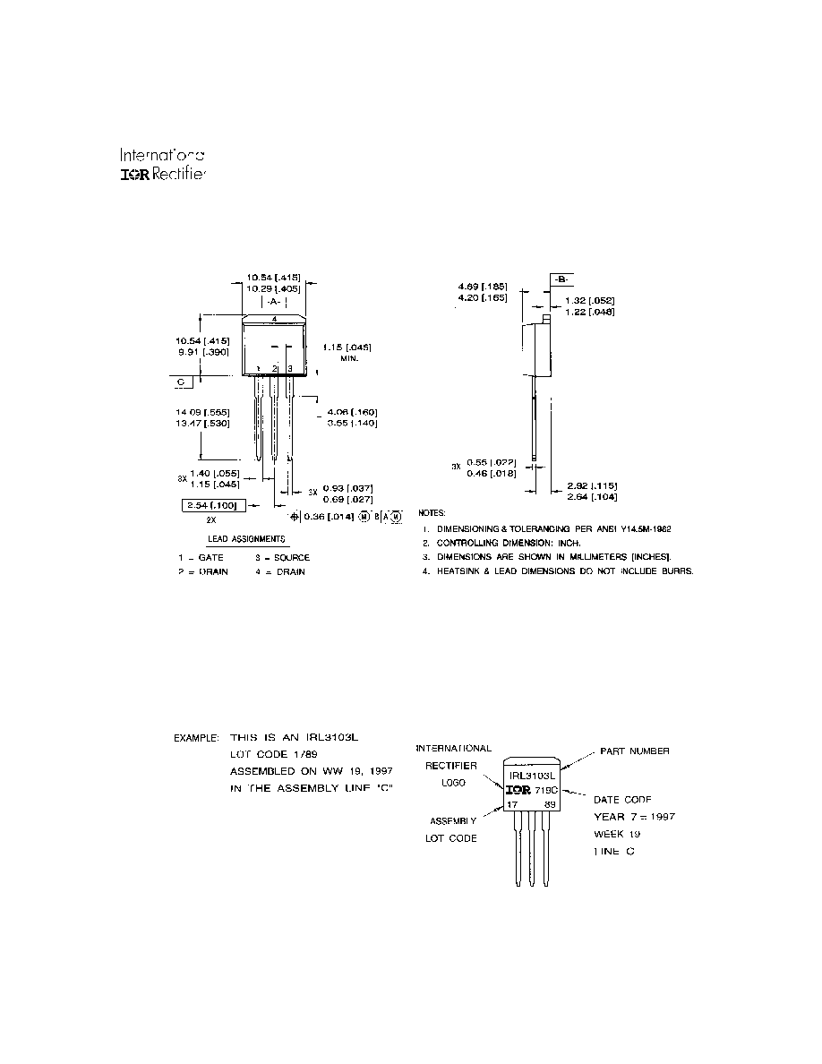
L E A D A S S IG N M E N T S
1 - G A T E
2 - D R A IN
3 - S O U R C E
4 - D R A IN
- B -
1 .3 2 ( .05 2 )
1 .2 2 ( .04 8 )
3 X
0.5 5 (.0 2 2 )
0.4 6 (.0 1 8 )
2 .9 2 ( .11 5 )
2 .6 4 ( .10 4 )
4 .6 9 ( .1 8 5 )
4 .2 0 ( .1 6 5 )
3 X
0 .93 ( .0 3 7 )
0 .69 ( .0 2 7 )
4 .0 6 ( .1 6 0 )
3 .5 5 ( .1 4 0 )
1 .1 5 ( .0 4 5 )
M IN
6 .4 7 (.2 5 5 )
6 .1 0 (.2 4 0 )
3 .7 8 (.1 4 9 )
3 .5 4 (.1 3 9 )
- A -
1 0 .5 4 ( .4 1 5 )
1 0 .2 9 ( .4 0 5 )
2 .8 7 ( .1 1 3 )
2 .6 2 ( .1 0 3 )
1 5 .2 4 ( .6 0 0 )
1 4 .8 4 ( .5 8 4 )
1 4 .0 9 ( .5 5 5 )
1 3 .4 7 ( .5 3 0 )
3 X
1 .4 0 (.0 5 5 )
1 .1 5 (.0 4 5 )
2 .5 4 ( .1 0 0 )
2 X
0 .3 6 ( .0 1 4 ) M B A M
4
1 2 3
N O T E S :
1 D IM E N S IO N IN G & T O L E R A N C IN G P E R A N S I Y 1 4 .5 M , 1 9 8 2 . 3 O U T L IN E C O N F O R M S T O J E D E C O U T L IN E T O -2 2 0 A B .
2 C O N T R O L L IN G D IM E N S IO N : IN C H 4 H E A T S IN K & L E A D M E A S U R E M E N T S D O N O T IN C L U D E B U R R S .
TO-220AB Part Marking Information
TO-220AB Package Outline
Dimensions are shown in millimeters (inches)
P A R T N U M B E R
IN T E R N A T IO N A L
R E C T IF IE R
L O G O
E X A M P L E : T H IS IS A N IR F 1 0 1 0
W IT H A S S E M B L Y
L O T C O D E 9 B 1 M
A S S E M B L Y
L O T C O D E
D A T E C O D E
(Y Y W W )
Y Y = Y E A R
W W = W E E K
9 2 4 6
IR F 1 0 1 0
9 B 1 M
A
IRF3707/3707S/3707L
8
www.irf.com
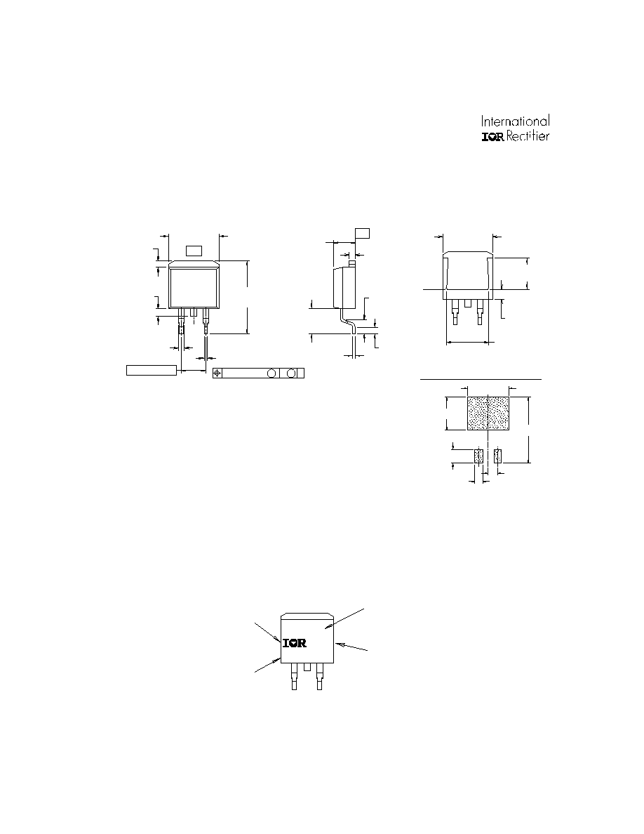
D
2
Pak Package Outline
D
2
Pak Part Marking Information
10 .1 6 (.4 00 )
R E F .
6.47 (.2 55 )
6.18 (.2 43 )
2.61 (.1 03 )
2.32 (.0 91 )
8.8 9 (.3 50 )
R E F .
- B -
1.3 2 (.05 2)
1.2 2 (.04 8)
2.7 9 (.110 )
2.2 9 (.090 )
1.3 9 (.0 55 )
1.1 4 (.0 45 )
5.28 (.2 08 )
4.78 (.1 88 )
4 .6 9 (.18 5)
4 .2 0 (.16 5)
1 0.54 (.415 )
1 0.29 (.405 )
- A -
2
1 3
1 5.49 (.6 10)
1 4.73 (.5 80)
3X
0.9 3 (.0 37 )
0.6 9 (.0 27 )
5 .08 (.20 0)
3X
1.40 (.0 55)
1.14 (.0 45)
1.7 8 (.07 0)
1.2 7 (.05 0)
1.4 0 (.055 )
M AX.
NO TE S:
1 D IM EN S IO N S A F T ER SO LD E R D IP .
2 D IM EN S IO N IN G & T O LE R AN C IN G P ER AN S I Y1 4.5M , 19 82 .
3 C O N T RO L LIN G D IM EN S IO N : IN C H.
4 H E AT SINK & L EA D D IM E N SIO N S DO N O T IN C LU D E B U R RS .
0.55 (.0 22)
0.46 (.0 18)
0.25 (.0 10 ) M B A M
M IN IM U M R EC O M M E ND E D F O O TP R IN T
1 1.43 (.4 50 )
8 .89 (.35 0)
17 .78 (.70 0)
3.81 (.1 5 0)
2.0 8 (.08 2)
2 X
LE AD AS SIG N M E N TS
1 - G AT E
2 - D RA IN
3 - SO U R C E
2.5 4 (.100 )
2 X
P A R T N U M B E R
IN TE R N A TIO N A L
R E C T IF IE R
L O G O
D A T E C O D E
(Y YW W )
YY = Y E A R
W W = W E E K
A S S E M B L Y
L O T C O D E
F 5 3 0 S
9 B 1 M
9 24 6
A
Dimensions are shown in millimeters (inches)
IRF3707/3707S/3707L
www.irf.com
9
TO-262 Part Marking Information
TO-262 Package Outline
Dimensions are shown in millimeters (inches)
IRF3707/3707S/3707L
10
www.irf.com
IR WORLD HEADQUARTERS: 233 Kansas St., El Segundo, California 90245, USA Tel: (310) 252-7105
IR EUROPEAN REGIONAL CENTRE: 439/445 Godstone Rd, Whyteleafe, Surrey CR3 OBL, UK Tel: ++ 44 (0)20 8645 8000
IR CANADA: 15 Lincoln Court, Brampton, Ontario L6T3Z2, Tel: (905) 453 2200
IR GERMANY: Saalburgstrasse 157, 61350 Bad Homburg Tel: ++ 49 (0) 6172 96590
IR ITALY: Via Liguria 49, 10071 Borgaro, Torino Tel: ++ 39 011 451 0111
IR JAPAN: K&H Bldg., 2F, 30-4 Nishi-Ikebukuro 3-Chome, Toshima-Ku, Tokyo 171 Tel: 81 (0)3 3983 0086
IR SOUTHEAST ASIA: 1 Kim Seng Promenade, Great World City West Tower, 13-11, Singapore 237994 Tel: ++ 65 (0)838 4630
IR TAIWAN:16 Fl. Suite D. 207, Sec. 2, Tun Haw South Road, Taipei, 10673 Tel: 886-(0)2 2377 9936
Data and specifications subject to change without notice. 8/00
Repetitive rating; pulse width limited by
max. junction temperature.
Notes:
Starting T
J
= 25°C, L = 0.7 mH
R
G
= 25
, I
AS
= 24.8 A.
Pulse width
300µs; duty cycle
2%.
Dimensions are shown in millimeters (inches)
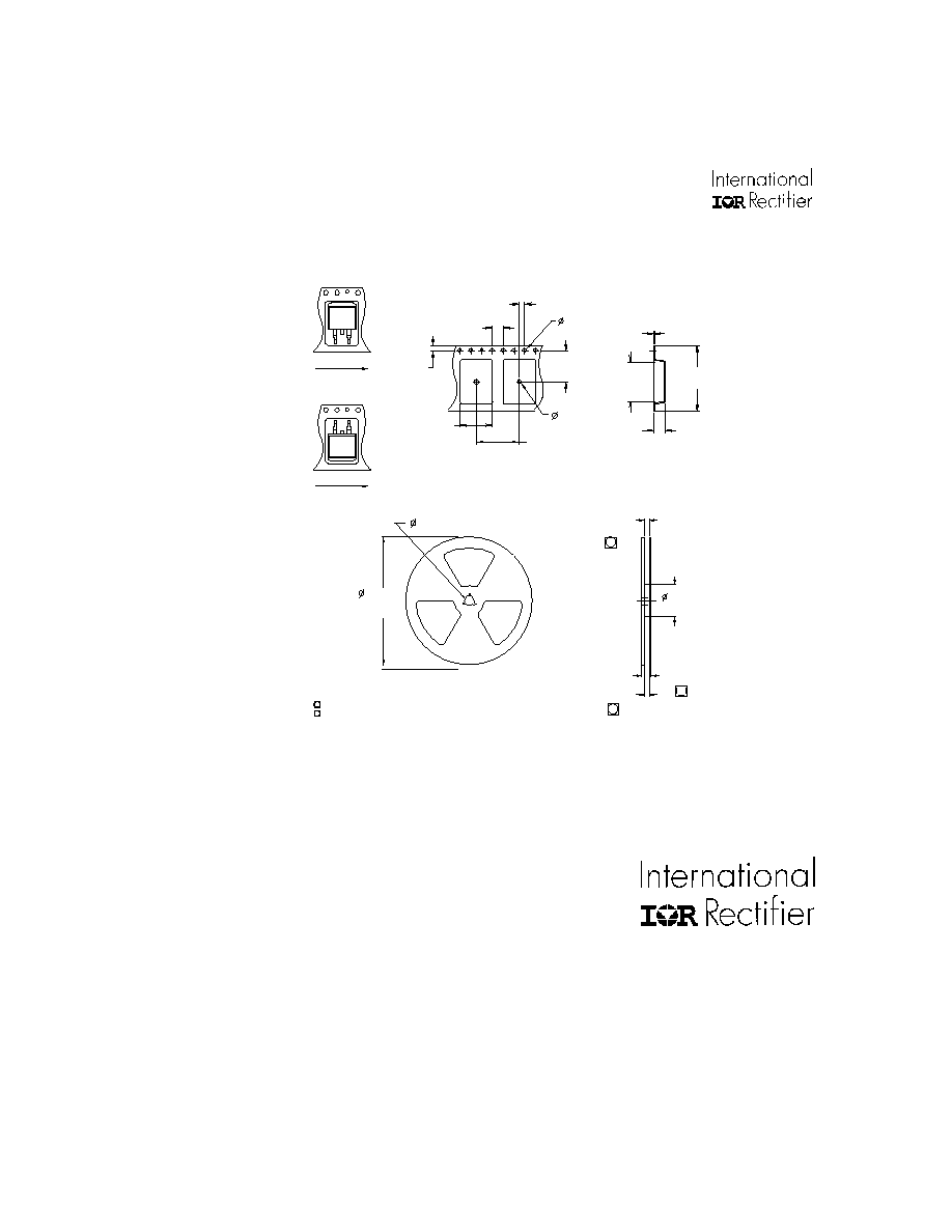
D
2
Pak Tape & Reel Information
3
4
4
T R R
F E E D D IR E C T IO N
1 .8 5 (.0 7 3 )
1 .6 5 (.0 6 5 )
1 .6 0 (.0 63 )
1 .5 0 (.0 59 )
4 .1 0 ( .1 6 1)
3 .9 0 ( .1 5 3)
T R L
F E E D D IR E C T IO N
10 .9 0 (.42 9)
10 .7 0 (.42 1)
16 .1 0 (.63 4)
15 .9 0 (.62 6)
1.75 (.0 69 )
1.25 (.0 49 )
1 1.60 (.457 )
1 1.40 (.449 )
15 .4 2 (.60 9)
15 .2 2 (.60 1)
4 .7 2 (.13 6)
4 .5 2 (.17 8)
24.30 (.95 7)
23.90 (.94 1)
0 .3 68 (.0 145 )
0 .3 42 (.0 135 )
1.60 (.06 3)
1.50 (.05 9)
13.50 (.532)
12.80 (.504)
33 0.00
(14.173)
M AX .
27.40 (1.079)
23.90 (.941)
60.00 (2.362)
M IN.
30.40 (1.197)
MA X.
26.40 (1.039)
24.40 (.961)
NO TE S :
1. CO MF OR M S TO EIA-418.
2. CO N TRO LLIN G DIM ENSIO N : MILLIM ET ER .
3. DIM ENS ION MEAS URED @ HU B.
4. INC LUD ES FLAN GE DIS TO RTIO N @ OU TER ED G E.
This is only applied to TO-220AB package