 | ÐлекÑÑоннÑй компоненÑ: IRF3709S | СкаÑаÑÑ:  PDF PDF  ZIP ZIP |
Äîêóìåíòàöèÿ è îïèñàíèÿ www.docs.chipfind.ru
www.irf.com
1
02/20/01
Symbol
Parameter
Max.
Units
V
DS
Drain-Source Voltage
30
V
V
GS
Gate-to-Source Voltage
± 20 V
I
D
@ T
C
= 25°C
Continuous Drain Current, V
GS
@ 10V
90
I
D
@ T
C
= 100°C
Continuous Drain Current, V
GS
@ 10V
57
A
I
DM
Pulsed Drain Current
360
P
D
@T
C
= 25°C
Maximum Power Dissipation
120
W
P
D
@T
A
= 25°C
Maximum Power Dissipation
3.1
W
Linear Derating Factor 0.96
mW/°C
T
J
, T
STG
Junction and Storage Temperature Range
-55 to + 150
°C
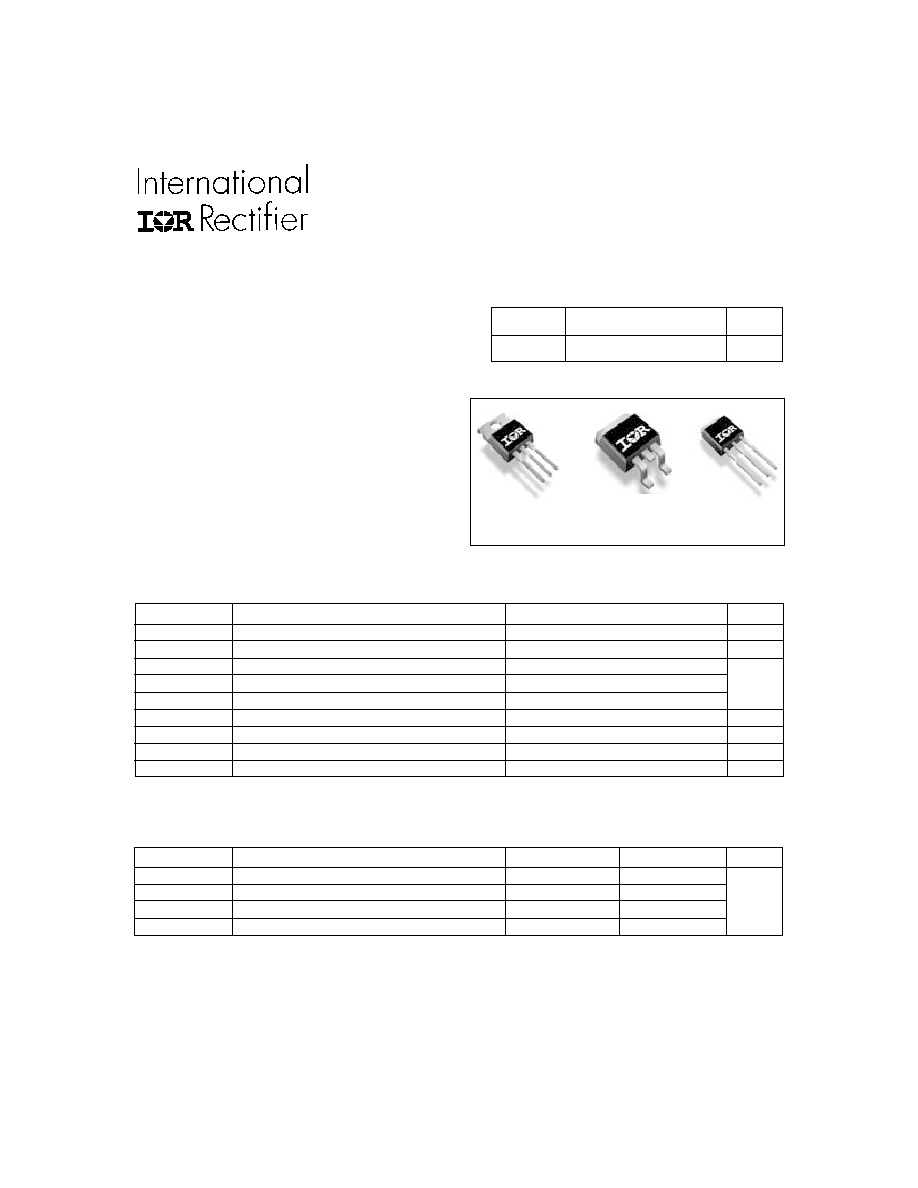
IRF3709
IRF3709S
IRF3709L
SMPS MOSFET
HEXFET
®
Power MOSFET
V
DSS
R
DS(on)
max
I
D
30V
9.0m
90A
Notes
through
are on page 11
Absolute Maximum Ratings
D
2
Pak
IRF3709S
TO-220AB
IRF3709
TO-262
IRF3709L
Thermal Resistance
Parameter
Typ.
Max.
Units
R
JC
Junction-to-Case
1.04
R
CS
Case-to-Sink, Flat, Greased Surface
0.50
°C/W
R
JA
Junction-to-Ambient
62
R
JA
Junction-to-Ambient (PCB mount)
40
Applications
Benefits
l
Ultra-Low Gate Impedance
l
Very Low RDS(on) at 4.5V V
GS
l
Fully Characterized Avalanche Voltage
and Current
l
High Frequency Isolated DC-DC
Converters with Synchronous Rectification
for Telecom and Industrial Use
l
High Frequency Buck Converters for
Server Processor Power Synchronous FET
l
Optimized for Synchronous Buck
Converters Including Capacitive Induced
Turn-on Immunity
PD - 94071
IRF3709/3709S/3709L
2
www.irf.com
Symbol
Parameter
Min. Typ. Max. Units
Conditions
I
S
Continuous Source Current
MOSFET symbol
(Body Diode)
showing the
I
SM
Pulsed Source Current
integral reverse
(Body Diode)
p-n junction diode.
0.88
1.3
V
T
J
= 25°C, I
S
= 30A, V
GS
= 0V
0.82
T
J
= 125°C, I
S
= 30A, V
GS
= 0V
t
rr
Reverse Recovery Time
48
72
ns
T
J
= 25°C, I
F
= 30A, V
R
=15V
Q
rr
Reverse Recovery Charge
46
69
nC
di/dt = 100A/µs
t
rr
Reverse Recovery Time
48
72
ns
T
J
= 125°C, I
F
= 30A, V
R
=15V
Q
rr
Reverse Recovery Charge
52
78
nC
di/dt = 100A/µs
Dynamic @ T
J
= 25°C (unless otherwise specified)
ns
Symbol
Parameter
Typ.
Max.
Units
E
AS
Single Pulse Avalanche Energy
382
mJ
I
AR
Avalanche Current
30
A
Avalanche Characteristics
S
D
G
Diode Characteristics
90
360
A
Symbol
Parameter
Min. Typ. Max. Units
Conditions
g
fs
Forward Transconductance
53
S
V
DS
= 15V, I
D
= 30A
Q
g
Total Gate Charge
27
41 I
D
= 15A
Q
gs
Gate-to-Source Charge
6.7
nC
V
DS
= 16V
Q
gd
Gate-to-Drain ("Miller") Charge
9.7
V
GS
= 5.0V
Q
oss
Output Gate Charge
22
V
GS
= 0V, V
DS
= 10V
t
d(on)
Turn-On Delay Time
11
V
DD
= 15V
t
r
Rise Time
171
I
D
= 30A
t
d(off)
Turn-Off Delay Time
21
R
G
= 1.8
t
f
Fall Time
9.2
V
GS
= 4.5V
C
iss
Input Capacitance
2672
V
GS
= 0V
C
oss
Output Capacitance
1064
pF
V
DS
= 16V
C
rss
Reverse Transfer Capacitance
109
= 1.0MHz
V
SD
Diode Forward Voltage
Parameter
Min. Typ. Max. Units
Conditions
V
(BR)DSS
Drain-to-Source Breakdown Voltage
30
V
V
GS
= 0V, I
D
= 250µA
V
(BR)DSS
/
T
J
Breakdown Voltage Temp. Coefficient
0.029 V/°C Reference to 25°C, I
D
= 1mA
6.4
9.0
V
GS
= 10V, I
D
= 15A
7.4
10.5
V
GS
= 4.5V, I
D
= 12A
V
GS(th)
Gate Threshold Voltage
1.0
3.0
V
V
DS
= V
GS
, I
D
= 250µA
20
µA
V
DS
= 24V, V
GS
= 0V
100
V
DS
= 24V, V
GS
= 0V, T
J
= 125°C
Gate-to-Source Forward Leakage
200
V
GS
= 16V
Gate-to-Source Reverse Leakage
-200
nA
V
GS
= -16V
Static @ T
J
= 25°C (unless otherwise specified)
I
GSS
I
DSS
Drain-to-Source Leakage Current
R
DS(on)
Static Drain-to-Source On-Resistance
m
IRF3709/3709S/3709L
www.irf.com
3
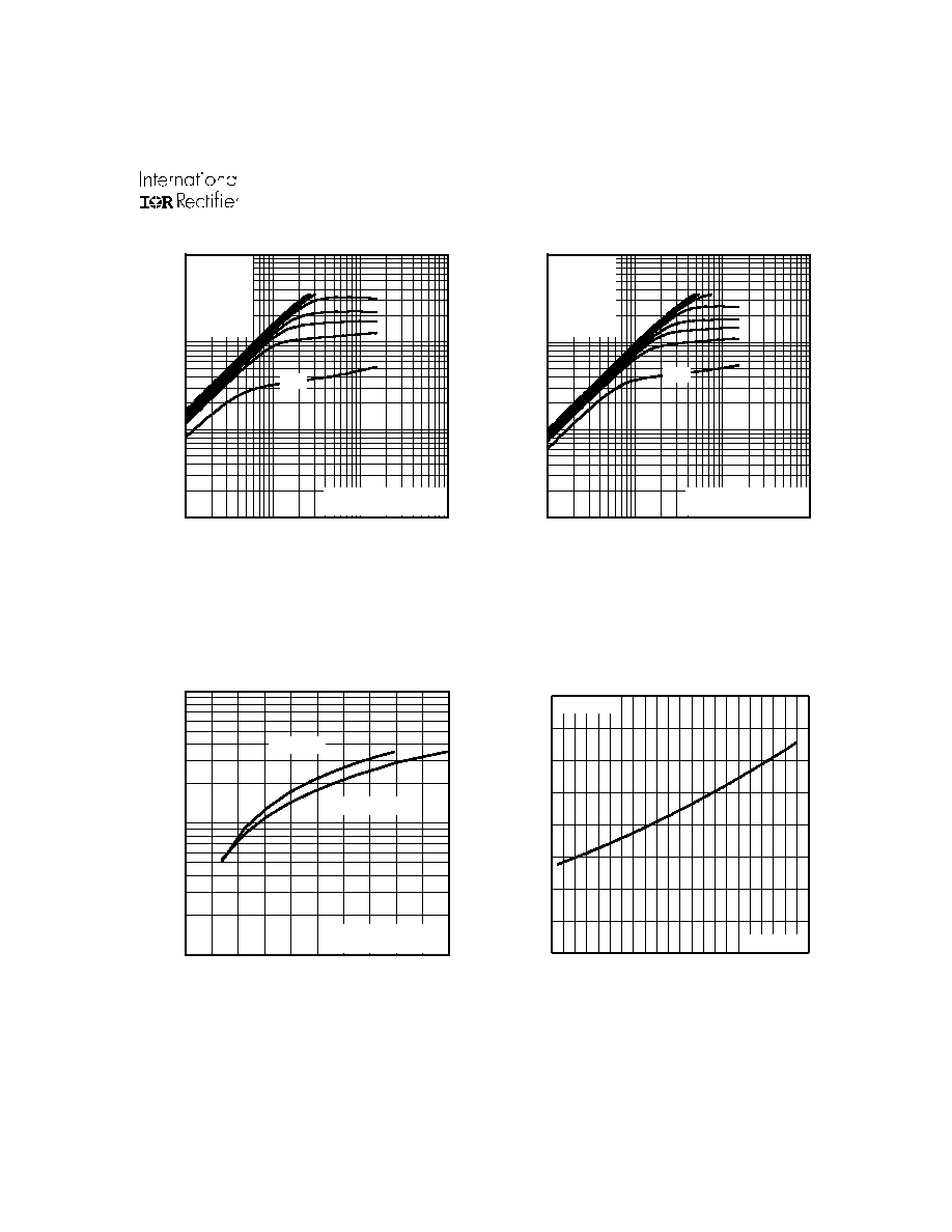
Fig 4. Normalized On-Resistance
Vs. Temperature
Fig 2. Typical Output Characteristics
Fig 1. Typical Output Characteristics
Fig 3. Typical Transfer Characteristics
10
100
1000
2.0
3.0
4.0
5.0
6.0
7.0
V = 15V
20µs PULSE WIDTH
DS
V , Gate-to-Source Voltage (V)
I , Drain-to-Source Current (A)
GS
D
T = 25 C
J
°
T = 150 C
J
°
-60 -40 -20
0
20
40
60
80 100 120 140 160
0.0
0.5
1.0
1.5
2.0
T , Junction Temperature ( C)
R , Drain-to-Source On Resistance
(Normalized)
J
DS(on)
°
V
=
I =
GS
D
10V
90A
1
10
100
1000
0.1
1
10
100
20µs PULSE WIDTH
T = 25 C
J
°
TOP
BOTTOM
VGS
15V
10V
7.0V
5.5V
4.5V
4.0V
3.5V
2.7V
V , Drain-to-Source Voltage (V)
I , Drain-to-Source Current (A)
DS
D
2.7V
1
10
100
1000
0.1
1
10
100
20µs PULSE WIDTH
T = 150 C
J
°
TOP
BOTTOM
VGS
15V
10V
7.0V
5.5V
4.5V
4.0V
3.5V
2.7V
V , Drain-to-Source Voltage (V)
I , Drain-to-Source Current (A)
DS
D
2.7V
IRF3709/3709S/3709L
4
www.irf.com
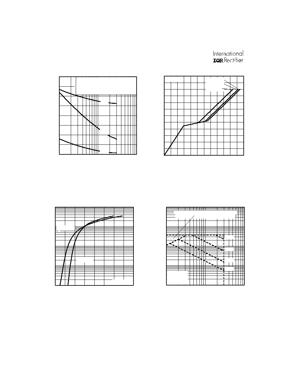
Fig 8. Maximum Safe Operating Area
Fig 6. Typical Gate Charge Vs.
Gate-to-Source Voltage
Fig 5. Typical Capacitance Vs.
Drain-to-Source Voltage
Fig 7. Typical Source-Drain Diode
Forward Voltage
0
5
10
15
20
25
30
0
1
2
3
4
5
6
Q , Total Gate Charge (nC)
V , Gate-to-Source Voltage (V)
G
GS
I =
D
30A
V
= 6V
DS
V
= 15V
DS
V
= 24V
DS
0.1
1
10
100
1000
0.2
0.8
1.4
2.0
2.6
V ,Source-to-Drain Voltage (V)
I , Reverse Drain Current (A)
SD
SD
V = 0 V
GS
T = 25 C
J
°
T = 150 C
J
°
1
10
100
1000
10000
1
10
100
OPERATION IN THIS AREA LIMITED
BY R
DS(on)
Single Pulse
T
T
= 150 C
= 25 C
°
°
J
C
V , Drain-to-Source Voltage (V)
I , Drain Current (A)
I , Drain Current (A)
DS
D
10us
100us
1ms
10ms
1
10
100
0
1000
2000
3000
4000
V , Drain-to-Source Voltage (V)
C, Capacitance (pF)
DS
V
C
C
C
=
=
=
=
0V,
C
C
C
f = 1MHz
+ C
+ C
C SHORTED
GS
iss
gs
gd ,
ds
rss
gd
oss
ds
gd
C
iss
C
oss
C
rss
IRF3709/3709S/3709L
www.irf.com
5
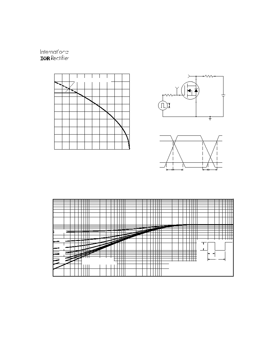
Fig 10a. Switching Time Test Circuit
V
DS
90%
10%
V
GS
t
d(on)
t
r
t
d(off)
t
f
Fig 10b. Switching Time Waveforms
V
DS
Pulse Width
1
µs
Duty Factor
0.1 %
R
D
V
GS
R
G
D.U.T.
V
GS
+
-
V
DD
Fig 11. Maximum Effective Transient Thermal Impedance, Junction-to-Case
Fig 9. Maximum Drain Current Vs.
Case Temperature
0.01
0.1
1
10
0.00001
0.0001
0.001
0.01
0.1
1
Notes:
1. Duty factor D = t / t
2. Peak T = P
x Z
+ T
1
2
J
DM
thJC
C
P
t
t
DM
1
2
t , Rectangular Pulse Duration (sec)
Thermal Response
(Z )
1
thJC
0.01
0.02
0.05
0.10
0.20
D = 0.50
SINGLE PULSE
(THERMAL RESPONSE)
25
50
75
100
125
150
0
20
40
60
80
100
T , Case Temperature
( C)
I , Drain Current (A)
°
C
D
LIMITED BY PACKAGE