 | –≠–ª–µ–∫—Ç—Ä–æ–Ω–Ω—ã–π –∫–æ–º–ø–æ–Ω–µ–Ω—Ç: IRF3808 | –°–∫–∞—á–∞—Ç—å:  PDF PDF  ZIP ZIP |

IRF3808
HEXFET
Æ
Power MOSFET
Designed specifically for Automotive applications, this Advanced
Planar Stripe HEXFET Æ Power MOSFET utilizes the latest process-
ing techniques to achieve extremely low on-resistance per silicon
area. Additional features of this HEXFET power MOSFET are a 175∞C
junction operating temperature, low R
JC, fast switching speed and
improved repetitive avalanche rating. This combination makes the
design an extremely efficient and reliable choice for use in higher
power Automotive electronic systems and a wide variety of other
applications.
S
D
G
Parameter
Max.
Units
I
D
@ T
C
= 25∞C
Continuous Drain Current, V
GS
@ 10V
140
V
I
D
@ T
C
= 100∞C
Continuous Drain Current, V
GS
@ 10V
97
V
A
I
DM
Pulsed Drain Current
Q
550
P
D
@T
C
= 25∞C
Power Dissipation
330
W
Linear Derating Factor
2.2
W/∞C
V
GS
Gate-to-Source Voltage
± 20
V
E
AS
Single Pulse Avalanche Energy
R
430
mJ
I
AR
Avalanche Current
Q
82
A
E
AR
Repetitive Avalanche Energy
W
See Fig.12a, 12b, 15, 16
mJ
dv/dt
Peak Diode Recovery dv/dt
S
5.5
V/ns
T
J
Operating Junction and
-55 to + 175
T
STG
Storage Temperature Range
Soldering Temperature, for 10 seconds
300 (1.6mm from case )
∞C
Mounting Torque, 6-32 or M3 screw
10 lbf∑in (1.1N∑m)
Absolute Maximum Ratings
Parameter
Typ.
Max.
Units
R
JC
Junction-to-Case
≠≠≠
0.45
R
CS
Case-to-Sink, Flat, Greased Surface
0.50
≠≠≠
∞C/W
R
JA
Junction-to-Ambient
≠≠≠
62
Thermal Resistance
V
DSS
= 75V
R
DS(on)
= 0.007
I
D
= 140A
V
Description
02/06/02
www.irf.com
1
q
Advanced Process Technology
q
Ultra Low On-Resistance
q
Dynamic dv/dt Rating
q
175∞C Operating Temperature
q
Fast Switching
q
Repetitive Avalanche Allowed up to Tjmax
Benefits
Typical Applications
q
Integrated Starter Alternator
q
42 Volts Automotive Electrical Systems
AUTOMOTIVE MOSFET
PD - 94291B
TO-220AB
HEXFET(R) is a registered trademark of International Rectifier.
IRF3808
2
www.irf.com
Parameter
Min. Typ. Max. Units
Conditions
V
(BR)DSS
Drain-to-Source Breakdown Voltage
75
≠≠≠
≠≠≠
V
V
GS
= 0V, I
D
= 250µA
V
(BR)DSS
/
T
J
Breakdown Voltage Temp. Coefficient
≠≠≠
0.086 ≠≠≠
V/∞C
Reference to 25∞C, I
D
= 1mA
R
DS(on)
Static Drain-to-Source On-Resistance
≠≠≠
5.9
7.0
m
V
GS
= 10V, I
D
= 82A
T
V
GS(th)
Gate Threshold Voltage
2.0
≠≠≠
4.0
V
V
DS
= 10V, I
D
= 250µA
g
fs
Forward Transconductance
100
≠≠≠
≠≠≠
S
V
DS
= 25V, I
D
= 82A
≠≠≠
≠≠≠
20
µA
V
DS
= 75V, V
GS
= 0V
≠≠≠
≠≠≠
250
V
DS
= 60V, V
GS
= 0V, T
J
= 150∞C
Gate-to-Source Forward Leakage
≠≠≠
≠≠≠
200
V
GS
= 20V
Gate-to-Source Reverse Leakage
≠≠≠
≠≠≠
-200
nA
V
GS
= -20V
Q
g
Total Gate Charge
≠≠≠
150
220
I
D
= 82A
Q
gs
Gate-to-Source Charge
≠≠≠
31
47
nC
V
DS
= 60V
Q
gd
Gate-to-Drain ("Miller") Charge
≠≠≠
50
76
V
GS
= 10V
T
t
d(on)
Turn-On Delay Time
≠≠≠
16
≠≠≠
V
DD
= 38V
t
r
Rise Time
≠≠≠
140
≠≠≠
I
D
= 82A
t
d(off)
Turn-Off Delay Time
≠≠≠
68
≠≠≠
R
G
= 2.5
t
f
Fall Time
≠≠≠
120
≠≠≠
V
GS
= 10V
T
Between lead,
≠≠≠
≠≠≠
6mm (0.25in.)
from package
and center of die contact
C
iss
Input Capacitance
≠≠≠
5310 ≠≠≠
V
GS
= 0V
C
oss
Output Capacitance
≠≠≠
890
≠≠≠
pF
V
DS
= 25V
C
rss
Reverse Transfer Capacitance
≠≠≠
130
≠≠≠
= 1.0MHz, See Fig. 5
C
oss
Output Capacitance
≠≠≠
6010 ≠≠≠
V
GS
= 0V, V
DS
= 1.0V, = 1.0MHz
C
oss
Output Capacitance
≠≠≠
570
≠≠≠
V
GS
= 0V, V
DS
= 60V, = 1.0MHz
C
oss
eff.
Effective Output Capacitance
U
≠≠≠
1140 ≠≠≠
V
GS
= 0V, V
DS
= 0V to 60V
nH
Electrical Characteristics @ T
J
= 25∞C (unless otherwise specified)
L
D
Internal Drain Inductance
L
S
Internal Source Inductance
≠≠≠
≠≠≠
S
D
G
I
GSS
ns
4.5
7.5
I
DSS
Drain-to-Source Leakage Current
Q
Repetitive rating; pulse width limited by
max. junction temperature. (See fig. 11).
R
Starting T
J
= 25∞C, L = 0.130mH
R
G
= 25
, I
AS
= 82A. (See Figure 12).
S
I
SD
82A, di/dt
310A/µs, V
DD
V
(BR)DSS
,
T
J
175∞C
T
Pulse width
400µs; duty cycle
2%.
Notes:
S
D
G
Parameter
Min. Typ. Max. Units
Conditions
I
S
Continuous Source Current
MOSFET symbol
(Body Diode)
≠≠≠
≠≠≠
showing the
I
SM
Pulsed Source Current
integral reverse
(Body Diode)
Q
≠≠≠
≠≠≠
p-n junction diode.
V
SD
Diode Forward Voltage
≠≠≠
≠≠≠
1.3
V
T
J
= 25∞C, I
S
= 82A, V
GS
= 0V
T
t
rr
Reverse Recovery Time
≠≠≠
93
140
ns
T
J
= 25∞C, I
F
= 82A
Q
rr
Reverse RecoveryCharge
≠≠≠
340
510
nC
di/dt = 100A/µs
T
t
on
Forward Turn-On Time
Intrinsic turn-on time is negligible (turn-on is dominated by L
S
+L
D
)
Source-Drain Ratings and Characteristics
140
V
550
A
U
C
oss
eff. is a fixed capacitance that gives the same charging time
as C
oss
while V
DS
is rising from 0 to 80% V
DSS
.
V
Calculated continuous current based on maximum allowable
junction temperature. Package limitation current is 75A.
W
Limited by T
Jmax
, see Fig.12a, 12b, 15, 16 for typical repetitive
avalanche performance.

IRF3808
www.irf.com
3
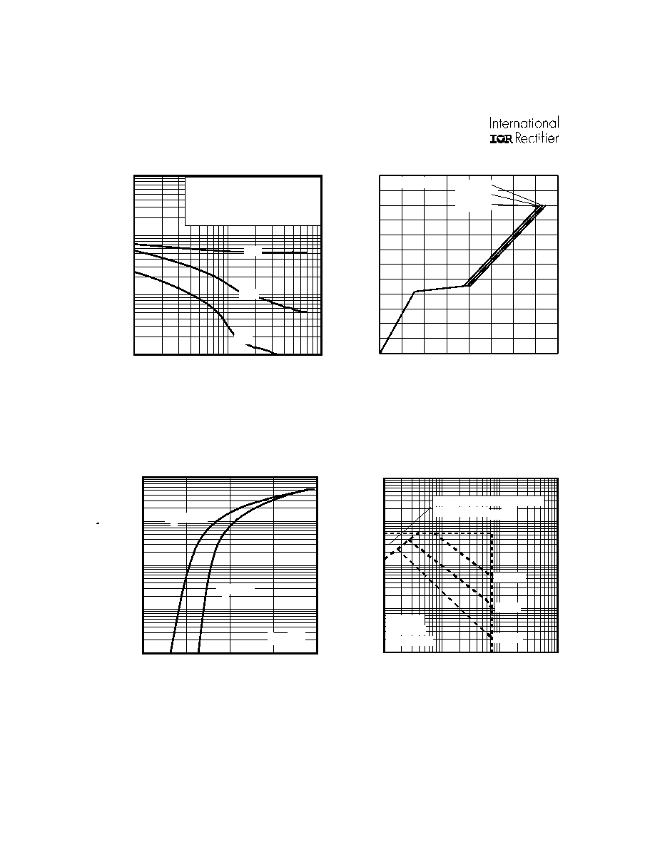
Fig 4. Normalized On-Resistance
Vs. Temperature
Fig 2. Typical Output Characteristics
Fig 1. Typical Output Characteristics
Fig 3. Typical Transfer Characteristics
1
10
100
1000
0.1
1
10
100
20µs PULSE WIDTH
T = 25
C
J
∞
TOP
BOTTOM
VGS
15V
10V
8.0V
7.0V
6.0V
5.5V
5.0V
4.5V
V , Drain-to-Source Voltage (V)
I , Drain-to-Source Current (A)
DS
D
4.5V
1
10
100
1000
0.1
1
10
100
20µs PULSE WIDTH
T = 175
C
J
∞
TOP
BOTTOM
VGS
15V
10V
8.0V
7.0V
6.0V
5.5V
5.0V
4.5V
V , Drain-to-Source Voltage (V)
I , Drain-to-Source Current (A)
DS
D
4.5V
-60
-40
-20
0
20
40
60
80
100
120
140
160
180
0.0
0.5
1.0
1.5
2.0
2.5
3.0
T , Junction Temperature
( C)
R , Drain-to-Source On Resistance
(Normalized)
J
DS(on)
∞
V
=
I
=
GS
D
10V
137A
1.0
3.0
5.0
7.0
9.0
11.0
13.0
15.0
VGS, Gate-to-Source Voltage (V)
10.00
100.00
1000.00
I D
, Drain-to-Source Current
(
)
TJ = 25∞C
TJ = 175∞C
VDS = 15V
20µs PULSE WIDTH
IRF3808
4
www.irf.com
Fig 8. Maximum Safe Operating Area
Fig 6. Typical Gate Charge Vs.
Gate-to-Source Voltage
Fig 5. Typical Capacitance Vs.
Drain-to-Source Voltage
Fig 7. Typical Source-Drain Diode
Forward Voltage
1
10
100
VDS, Drain-to-Source Voltage (V)
100
1000
10000
100000
C, Capacitance(pF)
Coss
Crss
Ciss
VGS = 0V, f = 1 MHZ
Ciss = Cgs + Cgd, Cds SHORTED
Crss = Cgd
Coss = Cds + Cgd
0.0
0.5
1.0
1.5
2.0
VSD, Source-toDrain Voltage (V)
0.10
1.00
10.00
100.00
1000.00
I SD
, Reverse Drain Current (A)
TJ = 25∞C
TJ = 175∞C
VGS = 0V
1
10
100
1000
VDS , Drain-toSource Voltage (V)
1
10
100
1000
10000
I D
, Drain-to-Source Current (A)
Tc = 25∞C
Tj = 175∞C
Single Pulse
1msec
10msec
OPERATION IN THIS AREA
LIMITED BY R DS(on)
100µsec
0
40
80
120
160
0
2
4
6
8
10
12
Q , Total Gate Charge (nC)
V , Gate-to-Source Voltage (V)
G
GS
I
=
D
82A
V
= 15V
DS
V
= 37V
DS
V
= 60V
DS

IRF3808
www.irf.com
5
Fig 9. Maximum Drain Current Vs.
Case Temperature
V
DS
90%
10%
V
GS
t
d(on)
t
r
t
d(off)
t
f
V
DS
Pulse Width
1
µs
Duty Factor
0.1 %
R
D
V
GS
R
G
D.U.T.
10V
+
-
V
DD
Fig 10a. Switching Time Test Circuit
Fig 10b. Switching Time Waveforms
Fig 11. Maximum Effective Transient Thermal Impedance, Junction-to-Case
25
50
75
100
125
150
175
0
20
40
60
80
100
120
140
T , Case Temperature
( C)
I , Drain Current (A)
∞
C
D
LIMITED BY PACKAGE
0.001
0.01
0.1
1
0.00001
0.0001
0.001
0.01
0.1
1
Notes:
1. Duty factor D =
t / t
2. Peak T
= P
x Z
+ T
1
2
J
DM
thJC
C
P
t
t
DM
1
2
t , Rectangular Pulse Duration (sec)
Thermal Response
(Z )
1
thJC
0.01
0.02
0.05
0.10
0.20
D = 0.50
SINGLE PULSE
(THERMAL RESPONSE)