 | ÐлекÑÑоннÑй компоненÑ: IRF520NS | СкаÑаÑÑ:  PDF PDF  ZIP ZIP |
Äîêóìåíòàöèÿ è îïèñàíèÿ www.docs.chipfind.ru
IRF520NS/L
HEXFET
®
Power MOSFET
PD -91340A
Fifth Generation HEXFETs from International Rectifier utilize advanced
processing techniques to achieve extremely low on-resistance per silicon area.
This benefit, combined with the fast switching speed and ruggedized device
design that HEXFET Power MOSFETs are well known for, provides the
designer with an extremely efficient and reliable device for use in a wide variety
of applications.
The D
2
Pak is a surface mount power package capable of accommodating die
sizes up to HEX-4. It provides the highest power capability and the lowest
possible on-resistance in any existing surface mount package. The D
2
Pak is
suitable for high current applications because of its low internal connection
resistance and can dissipate up to 2.0W in a typical surface mount application.
The through-hole version (IRF520NL) is available for low-profile applications.
S
D
G
Description
5/13/98
Parameter
Typ.
Max.
Units
R
JC
Junction-to-Case
3.1
R
JA
Junction-to-Ambient ( PCB Mounted,steady-state)**
40
Thermal Resistance
°C/W
Parameter
Max.
Units
I
D
@ T
C
= 25°C
Continuous Drain Current, V
GS
@ 10V
9.7
I
D
@ T
C
= 100°C
Continuous Drain Current, V
GS
@ 10V
6.8
A
I
DM
Pulsed Drain Current
38
P
D
@T
A
= 25°C
Power Dissipation
3.8
W
P
D
@T
C
= 25°C
Power Dissipation
48
W
Linear Derating Factor
0.32
W/°C
V
GS
Gate-to-Source Voltage
± 20
V
E
AS
Single Pulse Avalanche Energy
91
mJ
I
AR
Avalanche Current
5.7
A
E
AR
Repetitive Avalanche Energy
4.8
mJ
dv/dt
Peak Diode Recovery dv/dt
5.0
V/ns
T
J
Operating Junction and
-55 to + 175
T
STG
Storage Temperature Range
Soldering Temperature, for 10 seconds
300 (1.6mm from case )
°C
Absolute Maximum Ratings
l
Advanced Process Technology
l
Surface Mount (IRF520NS)
l
Low-profile through-hole (IRF520NL)
l
175°C Operating Temperature
l
Fast Switching
l
Fully Avalanche Rated
2
D P ak
T O -26 2
V
DSS
= 100V
R
DS(on)
= 0.20
I
D
= 9.7A
IRF520NS/L
Parameter
Min. Typ. Max. Units
Conditions
V
(BR)DSS
Drain-to-Source Breakdown Voltage
100
V
V
GS
= 0V, I
D
= 250µA
V
(BR)DSS
/
T
J
Breakdown Voltage Temp. Coefficient
0.11
V/°C
Reference to 25°C, I
D
= 1mA
R
DS(on)
Static Drain-to-Source On-Resistance
0.20
V
GS
= 10V, I
D
= 5.7A
V
GS(th)
Gate Threshold Voltage
2.0
4.0
V
V
DS
= V
GS
, I
D
= 250µA
g
fs
Forward Transconductance
2.7
S
V
DS
= 25V, I
D
= 5.7A
25
µA
V
DS
= 100V, V
GS
= 0V
250
V
DS
= 80V, V
GS
= 0V, T
J
= 150°C
Gate-to-Source Forward Leakage
100
V
GS
= 20V
Gate-to-Source Reverse Leakage
-100
nA
V
GS
= -20V
Q
g
Total Gate Charge
25
I
D
= 5.7A
Q
gs
Gate-to-Source Charge
4.8
nC
V
DS
= 80V
Q
gd
Gate-to-Drain ("Miller") Charge
11
V
GS
= 10V, See Fig. 6 and 13
t
d(on)
Turn-On Delay Time
4.5
V
DD
= 50V
t
r
Rise Time
23
I
D
= 5.7A
t
d(off)
Turn-Off Delay Time
32
R
G
= 22
t
f
Fall Time
23
R
D
= 8.6
,
See Fig. 10
Between lead,
and center of die contact
C
iss
Input Capacitance
330
V
GS
= 0V
C
oss
Output Capacitance
92
pF
V
DS
= 25V
C
rss
Reverse Transfer Capacitance
54
= 1.0MHz, See Fig. 5
Electrical Characteristics @ T
J
= 25°C (unless otherwise specified)
I
GSS
ns
I
DSS
Drain-to-Source Leakage Current
nH
7.5
L
S
Internal Source Inductance
V
DD
= 25V, starting T
J
= 25°C, L = 4.7mH
R
G
= 25
, I
AS
= 5.7A. (See Figure 12)
Repetitive rating; pulse width limited by
max. junction temperature. ( See fig. 11 )
Notes:
** When mounted on FR-4 board using minimum recommended footprint.
For recommended footprint and soldering techniques refer to application note #AN-994.
I
SD
5.7A, di/dt
240A/µs, V
DD
V
(BR)DSS
,
T
J
175°C
Pulse width
300µs; duty cycle
2%.
Uses IRF520N data and test conditions
Parameter
Min. Typ. Max. Units
Conditions
I
S
Continuous Source Current
MOSFET symbol
(Body Diode)
showing the
I
SM
Pulsed Source Current
integral reverse
(Body Diode)
p-n junction diode.
V
SD
Diode Forward Voltage
1.3
V
T
J
= 25°C, I
S
= 5.7A, V
GS
= 0V
t
rr
Reverse Recovery Time
99
150
ns
T
J
= 25°C, I
F
= 5.7A
Q
rr
Reverse RecoveryCharge
390
580
nC
di/dt = 100A/µs
Source-Drain Ratings and Characteristics
S
D
G
A
9.7
38
t
on
Forward Turn-On Time
Intrinsic turn-on time is negligible (turn-on is dominated by L
S
+L
D
)
IRF520NS/L
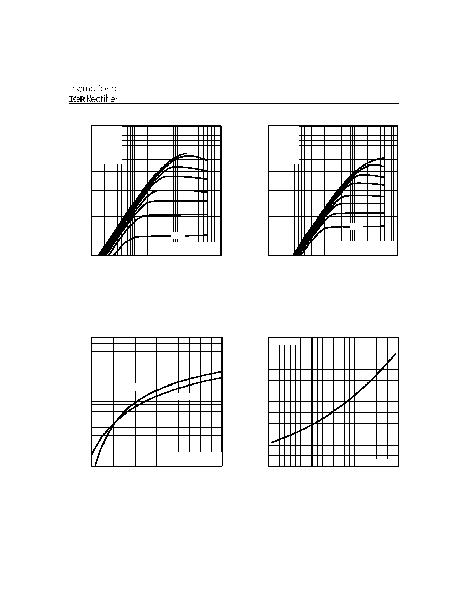
Fig 1. Typical Output Characteristics
Fig 3. Typical Transfer Characteristics
Fig 4. Normalized On-Resistance
Vs. Temperature
Fig 2. Typical Output Characteristics
1
1 0
1 0 0
0.1
1
1 0
1 0 0
I , D
r
a
i
n
-
to
-
S
o
u
r
c
e
C
u
r
r
e
n
t
(
A
)
D
V , D rain-to-S ource V o ltage (V )
D S
VGS
TO P 15V
10V
8.0V
7.0V
6.0V
5.5V
5.0V
BO TTOM 4.5V
2 0µ s P U L S E W ID T H
T = 25 °C
C
A
4 .5V
1
1 0
1 0 0
0.1
1
1 0
1 0 0
4 .5V
I
,
D
r
ai
n
-
t
o
-
S
ou
r
c
e Cur
r
e
nt
(
A
)
D
V , D rain-to-S ource V oltage (V )
DS
VGS
TOP 15V
10V
8.0V
7.0V
6.0V
5.5V
5.0V
BOTTOM 4.5V
2 0µ s P U L S E W ID T H
T = 17 5°C
C
A
1
1 0
1 0 0
4
5
6
7
8
9
1 0
T = 25 °C
J
G S
V , G ate-to -S o urce V oltag e (V )
D
I
,
D
r
a
i
n
-
t
o
-
S
o
u
rc
e
C
u
rre
n
t
(A
)
V = 5 0V
2 0µ s P U L S E W ID TH
DS
T = 1 7 5°C
J
A
0 . 0
0 . 5
1 . 0
1 . 5
2 . 0
2 . 5
3 . 0
- 6 0
- 4 0
- 2 0
0
2 0
4 0
6 0
8 0
1 0 0 1 2 0 1 4 0 1 6 0 1 8 0
J
T , Junction T em perature (°C )
R
, D
r
a
i
n
-
to
-
S
o
u
r
c
e
O
n
R
e
s
i
s
ta
n
c
e
D
S
(
on)
(N
o
r
m
a
l
i
z
e
d
)
V = 10 V
G S
A
I = 9 .5A
D
IRF520NS/L
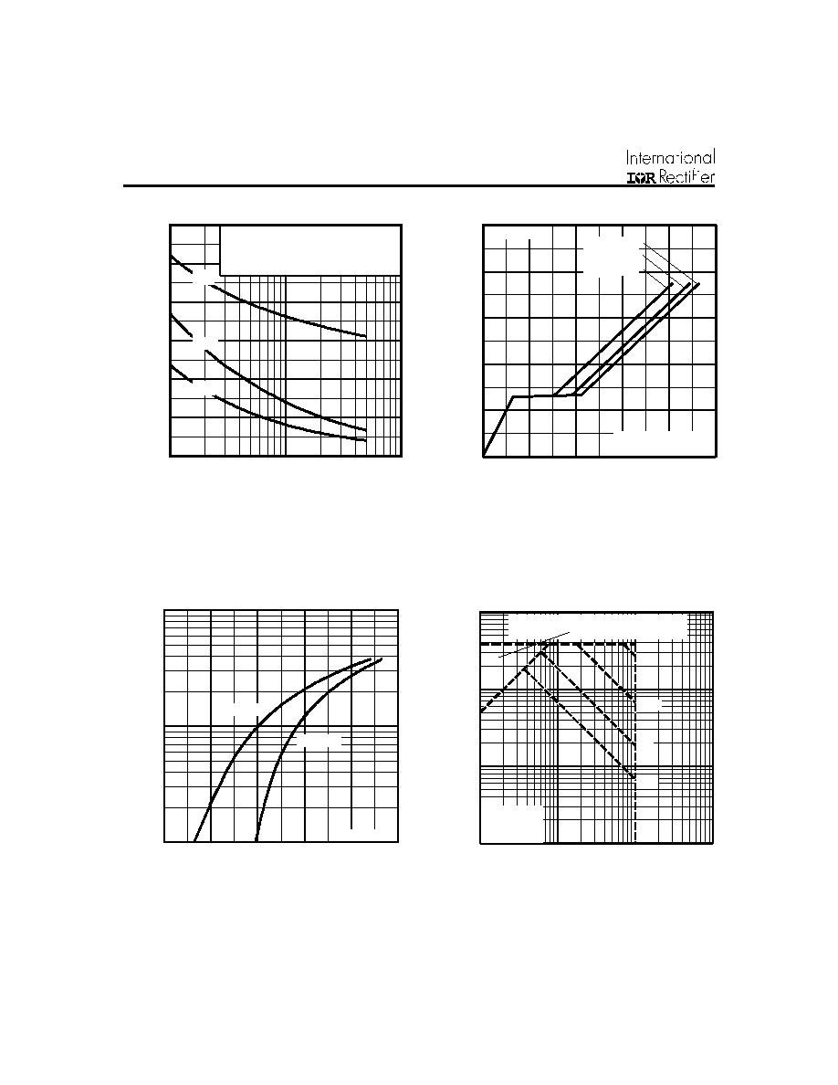
Fig 7. Typical Source-Drain Diode
Forward Voltage
Fig 5. Typical Capacitance Vs.
Drain-to-Source Voltage
Fig 8. Maximum Safe Operating Area
Fig 6. Typical Gate Charge Vs.
Gate-to-Source Voltage
0
1 0 0
2 0 0
3 0 0
4 0 0
5 0 0
6 0 0
1
1 0
1 0 0
C
,
Cap
ac
i
t
a
n
c
e
(
p
F
)
D S
V , D rain-to-S ourc e V oltage (V )
A
V = 0V , f = 1M H z
C = C + C , C S H O R T E D
C = C
C = C + C
G S
is s g s g d d s
rs s g d
o ss d s gd
C
iss
C
os s
C
rs s
0
4
8
1 2
1 6
2 0
0
5
1 0
1 5
2 0
2 5
Q , T otal G ate C harge (nC )
G
V
, G
a
te
-
t
o
-
S
o
u
r
c
e
V
o
l
t
a
g
e
(
V
)
GS
V = 80 V
V = 50 V
V = 20 V
D S
D S
D S
A
F O R TE S T C IR C U IT
S E E F IG U R E 1 3
I = 5.7 A
D
1
1 0
1 0 0
0 . 4
0 . 6
0 . 8
1 . 0
1 . 2
1 . 4
T = 2 5°C
J
V = 0V
G S
V , S ourc e-to-D ra in V oltage (V )
I , R
e
v
e
r
s
e
D
r
a
i
n
C
u
r
r
e
n
t
(
A
)
S D
SD
A
T = 17 5°C
J
0.1
1
1 0
1 0 0
1
1 0
1 0 0
1 0 0 0
V , D rain-to-S ource V oltage (V )
D S
I
,
Dr
ai
n
C
u
r
r
e
nt
(
A
)
O P E R A T IO N IN T H IS A R E A LIM IT E D
B Y R
D
D S (o n)
1 0 µ s
1 0 0 µ s
1 m s
1 0 m s
A
T = 25 °C
T = 17 5°C
S ing le P u ls e
C
J
IRF520NS/L
Fig 9. Maximum Drain Current Vs.
Case Temperature
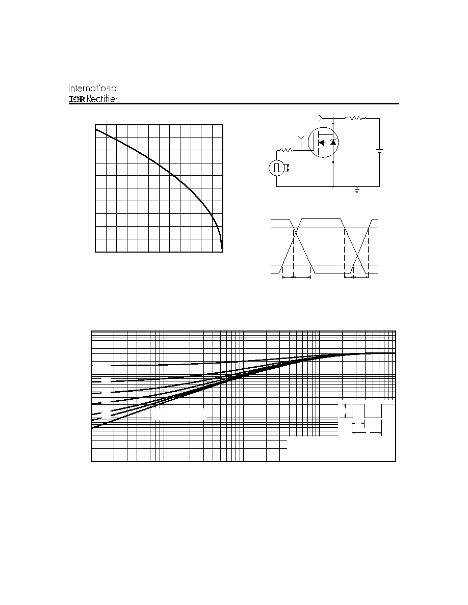
Fig 10a. Switching Time Test Circuit
V
DS
90%
10%
V
GS
t
d(on)
t
r
t
d(off)
t
f
Fig 10b. Switching Time Waveforms
Fig 11. Maximum Effective Transient Thermal Impedance, Junction-to-Case
V
DS
Pulse Width
1
µs
Duty Factor
0.1 %
R
D
V
GS
R
G
D.U.T.
10V
+
-
V
DD
25
50
75
100
125
150
175
0.0
2.0
4.0
6.0
8.0
10.0
T , Case Temperature
( C)
I , Drain Current (A)
°
C
D
0.01
0.1
1
10
0.00001
0.0001
0.001
0.01
0.1
Notes:
1. Duty factor D =
t / t
2. Peak T = P
x Z
+ T
1
2
J
DM
thJC
C
P
t
t
DM
1
2
t , Rectangular Pulse Duration (sec)
Thermal Response
(Z )
1
thJC
0.01
0.02
0.05
0.10
0.20
D = 0.50
SINGLE PULSE
(THERMAL RESPONSE)