 | ÐлекÑÑоннÑй компоненÑ: IRF5800 | СкаÑаÑÑ:  PDF PDF  ZIP ZIP |
Äîêóìåíòàöèÿ è îïèñàíèÿ www.docs.chipfind.ru
Parameter
Max.
Units
V
DS
Drain- Source Voltage
-30
V
I
D
@ T
A
= 25°C
Continuous Drain Current, V
GS
@ -4.5V
-4.0
I
D
@ T
A
= 70°C
Continuous Drain Current, V
GS
@ -4.5V
-3.2
A
I
DM
Pulsed Drain Current
-32
P
D
@T
A
= 25°C
Power Dissipation
2.0
P
D
@T
A
= 70°C
Power Dissipation
1.3
Linear Derating Factor
0.016
W/°C
E
AS
Single Pulse Avalanche Energy
20.6
mJ
V
GS
Gate-to-Source Voltage
± 20
V
T
J,
T
STG
Junction and Storage Temperature Range
-55 to + 150
°C
2/8/00
Parameter
Max.
Units
R
JA
Maximum Junction-to-Ambient
62.5
°C/W
Thermal Resistance
Absolute Maximum Ratings
W
www.irf.com
1
IRF5800
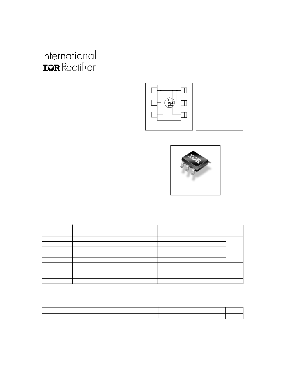
HEXFET
®
Power MOSFET
These P-channel MOSFETs from International Rectifier
utilize advanced processing techniques to achieve the
extremely low on-resistance per silicon area. This benefit
provides the designer with an extremely efficient device for
use in battery and load management applications.
The TSOP-6 package with its customized leadframe
produces a HEXFET
®
power MOSFET with R
DS(on)
60%
less than a similar size SOT-23. This package is ideal for
applications where printed circuit board space is at a
premium. It's unique thermal design and R
DS(on)
reduction
enables a current-handling increase of nearly 300%
compared to the SOT-23.
V
DSS
= -30V
R
DS(on)
= 0.085
Description
l
Ultra Low On-Resistance
l
P-Channel MOSFET
l
Surface Mount
l
Available in Tape & Reel
l
Low Gate Charge
T o p V ie w
1
2
D
G
A
D
D
D
S
3
4
5
6
PD - 93850
TSOP-6
IRF5800
2
www.irf.com
Parameter
Min. Typ. Max. Units
Conditions
I
S
Continuous Source Current
MOSFET symbol
(Body Diode)
showing the
I
SM
Pulsed Source Current
integral reverse
(Body Diode)
p-n junction diode.
V
SD
Diode Forward Voltage
-1.2
V
T
J
= 25°C, I
S
= -2.0A, V
GS
= 0V
t
rr
Reverse Recovery Time
19
28
ns
T
J
= 25°C, I
F
= -2.0A
Q
rr
Reverse Recovery Charge
16
24
nC
di/dt = -100A/µs
Source-Drain Ratings and Characteristics
A
-32
-2.0
S
D
G
Repetitive rating; pulse width limited by
max. junction temperature.
Notes:
Pulse width
300µs; duty cycle
2%.
Surface mounted on FR-4 board, t
5sec.
Starting T
J
= 25°C, L = 2.5mH
R
G
= 25
, I
AS
= -4.0A. (See Fig 10 )
Parameter
Min. Typ. Max. Units
Conditions
V
(BR)DSS
Drain-to-Source Breakdown Voltage
-30
V
V
GS
= 0V, I
D
= -250µA
V
(BR)DSS
/
T
J
Breakdown Voltage Temp. Coefficient
0.02
V/°C
Reference to 25°C, I
D
= 1mA
0.085
V
GS
= -10V, I
D
= -4.0A
0.150
V
GS
= -4.5V, I
D
= -3.0A
V
GS(th)
Gate Threshold Voltage
-1.0
V
V
DS
= V
GS
, I
D
= -250µA
g
fs
Forward Transconductance
3.5
S
V
DS
= -10V, I
D
= -4.0A
-1.0
V
DS
= -24V, V
GS
= 0V
-5.0
V
DS
= -24V, V
GS
= 0V, T
J
= 70°C
Gate-to-Source Forward Leakage
-100
V
GS
= -20V
Gate-to-Source Reverse Leakage
100
V
GS
= 20V
Q
g
Total Gate Charge
11.4
17
I
D
= -4.0A
Q
gs
Gate-to-Source Charge
2.3
nC
V
DS
= -16V
Q
gd
Gate-to-Drain ("Miller") Charge
2.2
V
GS
= -10V
t
d(on)
Turn-On Delay Time
11.4
17
V
DD
= -15V, V
GS
= -10V
t
r
Rise Time
11
17
I
D
= -1.0A
t
d(off)
Turn-Off Delay Time
24
36
R
G
= 6.0
t
f
Fall Time
14
20
R
D
= 15
,
C
iss
Input Capacitance
535
V
GS
= 0V
C
oss
Output Capacitance
94
pF
V
DS
= -25V
C
rss
Reverse Transfer Capacitance
68
= 1.0MHz
Electrical Characteristics @ T
J
= 25°C (unless otherwise specified)
I
GSS
µA
R
DS(on)
Static Drain-to-Source On-Resistance
I
DSS
Drain-to-Source Leakage Current
nA
ns
IRF5800
www.irf.com
3
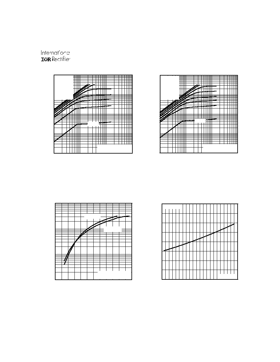
Fig 4. Normalized On-Resistance
Vs. Temperature
Fig 2. Typical Output Characteristics
Fig 1. Typical Output Characteristics
Fig 3. Typical Transfer Characteristics
0.01
0.1
1
10
100
0.1
1
10
100
20µs PULSE WIDTH
T = 25 C
J
°
TOP
BOTTOM
VGS
-15V
-10V
-7.0V
-5.5V
-4.5V
-4.0V
-3.5V
-2.7V
-V , Drain-to-Source Voltage (V)
-I , Drain-to-Source Current (A)
DS
D
-2.70V
0.01
0.1
1
10
100
0.1
1
10
100
20µs PULSE WIDTH
T = 150 C
J
°
TOP
BOTTOM
VGS
-15V
-10V
-7.0V
-5.5V
-4.5V
-4.0V
-3.5V
-2.7V
-V , Drain-to-Source Voltage (V)
-I , Drain-to-Source Current (A)
DS
D
-2.70V
0.1
1
10
100
2.0
3.0
4.0
5.0
6.0
7.0
8.0
V = -15V
20µs PULSE WIDTH
DS
-V , Gate-to-Source Voltage (V)
-I , Drain-to-Source Current (A)
GS
D
T = 25 C
J
°
T = 150 C
J
°
-60 -40 -20
0
20
40
60
80 100 120 140 160
0.0
0.5
1.0
1.5
2.0
T , Junction Temperature ( C)
R , Drain-to-Source On Resistance
(Normalized)
J
DS(on)
°
V
=
I =
GS
D
-10V
-4.0A
IRF5800
4
www.irf.com
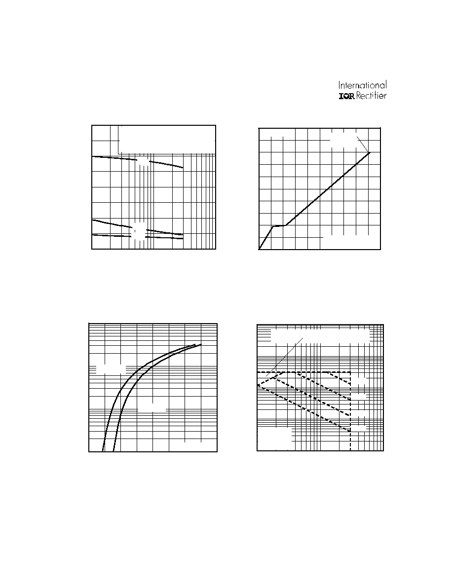
Fig 8. Maximum Safe Operating Area
Fig 6. Typical Gate Charge Vs.
Gate-to-Source Voltage
Fig 5. Typical Capacitance Vs.
Drain-to-Source Voltage
Fig 7. Typical Source-Drain Diode
Forward Voltage
1
10
100
0
200
400
600
800
-V , Drain-to-Source Voltage (V)
C, Capacitance (pF)
DS
V
C
C
C
=
=
=
=
0V,
C
C
C
f = 1MHz
+ C
+ C
C SHORTED
GS
iss
gs
gd ,
ds
rss
gd
oss
ds
gd
Crss
Coss
Ciss
0
4
8
12
16
20
0
4
8
12
16
20
Q , Total Gate Charge (nC)
-V , Gate-to-Source Voltage (V)
G
GS
FOR TEST CIRCUIT
SEE FIGURE
I =
D
13
-4.0A
V
= -16V
DS
0.1
1
10
100
0.4
0.8
1.2
1.6
2.0
-V ,Source-to-Drain Voltage (V)
-I , Reverse Drain Current (A)
SD
SD
V = 0 V
GS
T = 25 C
J
°
T = 150 C
J
°
0.1
1
10
100
1000
1
10
100
OPERATION IN THIS AREA LIMITED
BY R
DS(on)
Single Pulse
T
T
= 150 C
= 25 C
°
°
J
C
-V , Drain-to-Source Voltage (V)
-I , Drain Current (A)
I , Drain Current (A)
DS
D
10us
100us
1ms
10ms
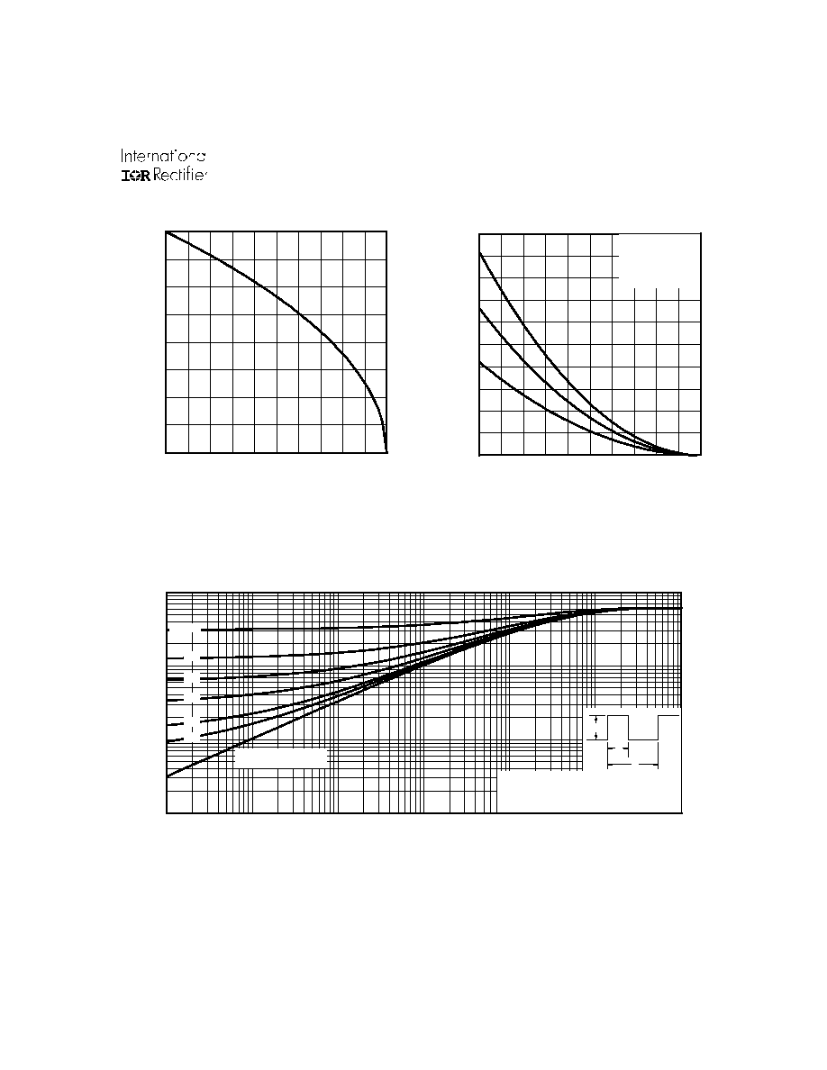
IRF5800
www.irf.com
5
Fig 11. Maximum Effective Transient Thermal Impedance, Junction-to-Ambient
Fig 9. Maximum Drain Current Vs.
Case Temperature
Fig 10. Maximum Avalanche Energy
Vs. Drain Current
25
50
75
100
125
150
0.0
1.0
2.0
3.0
4.0
T , Case Temperature
( C)
-I , Drain Current (A)
°
C
D
25
50
75
100
125
150
0
10
20
30
40
50
Starting T , Junction Temperature
( C)
E , Single Pulse Avalanche Energy (mJ)
J
AS
°
ID
TOP
BOTTOM
-1.8A
-2.5A
-4.0A
0.1
1
10
100
0.00001
0.0001
0.001
0.01
0.1
1
10
Notes:
1. Duty factor D = t / t
2. Peak T = P
x Z
+ T
1
2
J
DM
thJA
A
P
t
t
DM
1
2
t , Rectangular Pulse Duration (sec)
Thermal Response
(Z )
1
thJA
0.01
0.02
0.05
0.10
0.20
D = 0.50
SINGLE PULSE
(THERMAL RESPONSE)