 | ÐлекÑÑоннÑй компоненÑ: IRF5N3710 | СкаÑаÑÑ:  PDF PDF  ZIP ZIP |
Äîêóìåíòàöèÿ è îïèñàíèÿ www.docs.chipfind.ru
Absolute Maximum Ratings
Parameter
Units
ID @ VGS = 10V, TC = 25°C
Continuous Drain Current
45
ID @ VGS = 10V, TC = 100°C Continuous Drain Current
30
IDM
Pulsed Drain Current
180
PD @ TC = 25°C
Max. Power Dissipation
125
W
Linear Derating Factor
1.0
W/°C
VGS
Gate-to-Source Voltage
±20
V
EAS
Single Pulse Avalanche Energy
250
mJ
IAR
Avalanche Current
28
A
EAR
Repetitive Avalanche Energy
12.5
mJ
dv/dt
Peak Diode Recovery dv/dt
3.7
V/ns
T J
Operating Junction
-55 to 150
TSTG
Storage Temperature Range
Package Mounting Surface Temperature
300 (for 5 s)
Weight
2.6 (Typical)
g
o
C
A
7/9//01
www.irf.com
1
Product Summary
Part Number
BVDSS
R
DS(on)
I
D
IRF5N3710
100V
0.028
45A
For footnotes refer to the last page
HEXFET
®
POWER MOSFET
IRF5N3710
SURFACE MOUNT (SMD-1)
100V, N-CHANNEL
Fifth Generation HEXFET
®
power MOSFETs from
International Rectifier utilize advanced processing
techniques to achieve the lowest possible on-resistance
per silicon unit area. This benefit, combined with the
fast switching speed and ruggedized device design
that HEXFET power MOSFETs are well known for,
provides the designer with an extremely efficient device
for use in a wide variety of applications.
These devices are well-suited for applications such
as switching power supplies, motor controls, invert-
ers, choppers, audio amplifiers and high-energy pulse
circuits.
SMD-1
Features:
n
Low R
DS(on)
n
Avalanche Energy Ratings
n
Dynamic dv/dt Rating
n
Simple Drive Requirements
n
Ease of Paralleling
n
Hermetically Sealed
n
Surface Mount
n
Light Weight
PD - 94235A
IRF5N3710
2
www.irf.com
Electrical Characteristics
@ Tj = 25°C (Unless Otherwise Specified)
Parameter
Min
Typ Max Units
Test Conditions
BVDSS
Drain-to-Source Breakdown Voltage
100
--
--
V
VGS = 0V, ID = 250
µ
A
BVDSS/
TJ Temperature Coefficient of Breakdown
--
0.104
--
V/°C
Reference to 25°C, ID = 1.0mA
Voltage
RDS(on)
Static Drain-to-Source On-State
--
--
0.028
VGS = 10V, ID = 28A
Resistance
VGS(th)
Gate Threshold Voltage
2.0
--
4.0
V
VDS = VGS, ID = 250
µ
A
gfs
Forward Transconductance
20
--
--
S (
)
VDS =15V, IDS = 28A
IDSS
Zero Gate Voltage Drain Current
--
--
25
VDS = 100V ,VGS=0V
--
--
250
VDS = 80V,
VGS = 0V, TJ =125°C
IGSS
Gate-to-Source Leakage Forward
--
--
100
VGS =-20V
IGSS
Gate-to-Source Leakage Reverse
--
--
-100
VGS = -20V
Qg
Total Gate Charge
--
--
200
VGS =10V, ID = 28A
Qgs
Gate-to-Source Charge
--
--
28
nC
VDS = 80V
Qgd
Gate-to-Drain (`Miller') Charge
--
--
94
td
(on)
Turn-On Delay Time
--
--
25
VDD = 50V, ID = 28A,
tr
Rise Time
--
--
86
VGS = 10V, RG = 2.5
td
(off)
Turn-Off Delay Time
--
--
75
tf
Fall Time
--
--
54
LS + LD
Total Inductance
--
4.0
--
Measured from the center of
drain pad to center of source pad
Ciss
Input Capacitance
--
2920
--
VGS = 0V, VDS = 25V
Coss
Output Capacitance
--
700
--
pF
f = 1.0MHz
Crss
Reverse Transfer Capacitance
--
340
--
nA
nH
ns
µ
A
Thermal Resistance
Parameter
Min Typ Max
Units
Test Conditions
RthJC
Junction-to-Case
--
--
1.0
°C/W
Note: Corresponding Spice and Saber models are available on the G&S Website.
For footnotes refer to the last page
Source-Drain Diode Ratings and Characteristics
Parameter
Min Typ Max Units
Test Conditions
IS
Continuous Source Current (Body Diode)
--
--
45
ISM
Pulse Source Current (Body Diode)
--
--
180
VSD
Diode Forward Voltage
--
--
1.3
V
T
j
= 25°C, IS = 28A, VGS = 0V
trr
Reverse Recovery Time
--
--
280
ns
Tj = 25°C, IF = 28A, di/dt
100A/
µ
s
QRR
Reverse Recovery Charge
--
--
2.0
µ
C
VDD
50V
ton
Forward Turn-On Time
Intrinsic turn-on time is negligible. Turn-on speed is substantially controlled by LS + LD.
A
www.irf.com
3
IRF5N3710
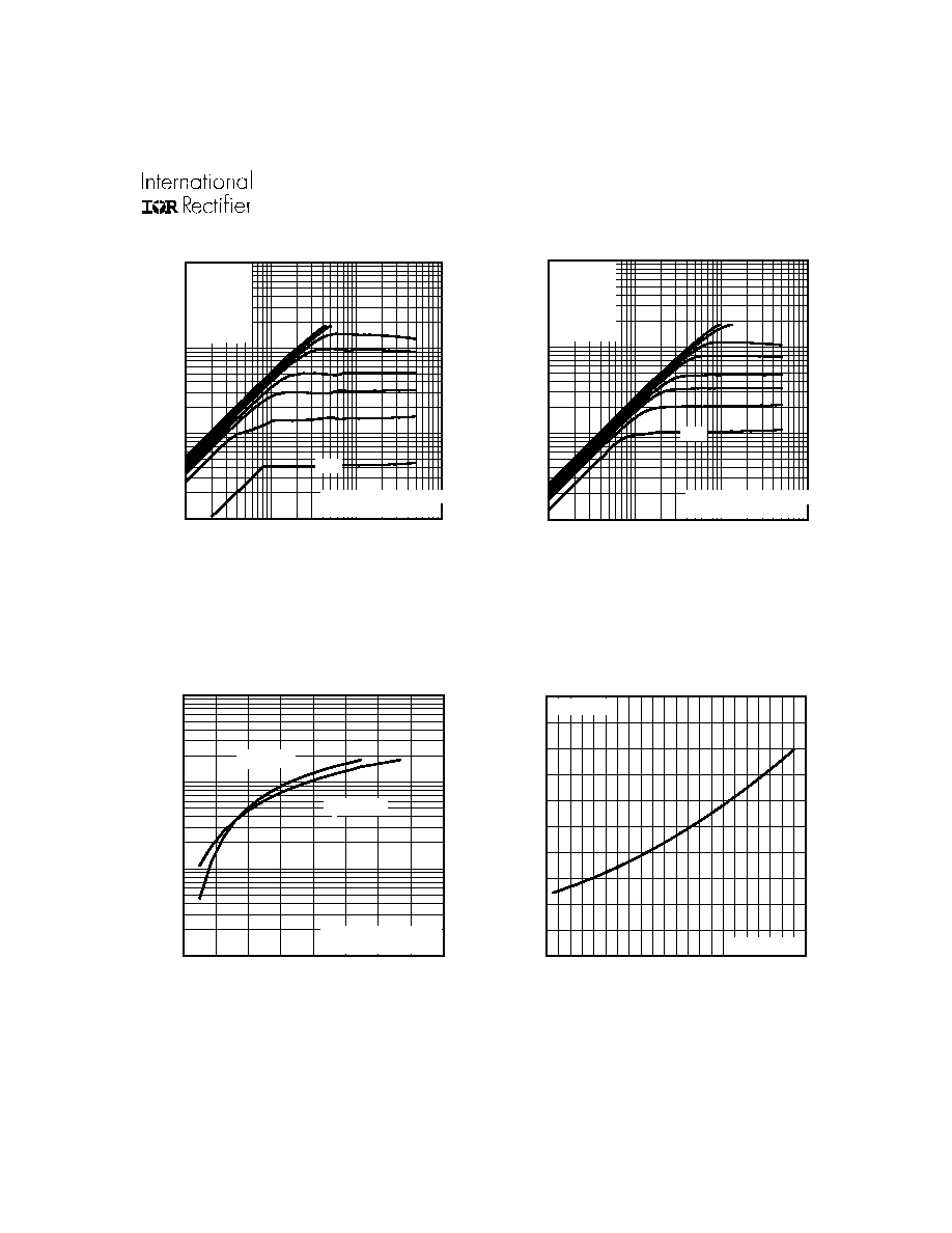
Fig 4. Normalized On-Resistance
Vs. Temperature
Fig 2. Typical Output Characteristics
Fig 1. Typical Output Characteristics
Fig 3. Typical Transfer Characteristics
15
1
10
100
1000
0.1
1
10
100
20µs PULSE WIDTH
T = 25 C
J
°
TOP
BOTTOM
VGS
15V
10V
8.0V
7.0V
6.0V
5.5V
5.0V
4.5V
V , Drain-to-Source Voltage (V)
I , Drain-to-Source Current (A)
DS
D
4.5V
1
10
100
1000
0.1
1
10
100
20µs PULSE WIDTH
T = 150 C
J
°
TOP
BOTTOM
VGS
15V
10V
8.0V
7.0V
6.0V
5.5V
5.0V
4.5V
V , Drain-to-Source Voltage (V)
I , Drain-to-Source Current (A)
DS
D
4.5V
1
10
100
1000
4
6
8
10
12
V = 50V
20µs PULSE WIDTH
DS
V , Gate-to-Source Voltage (V)
I , Drain-to-Source Current (A)
GS
D
T = 25 C
J
°
T = 150 C
J
°
-60 -40 -20
0
20
40
60
80 100 120 140 160
0.0
0.5
1.0
1.5
2.0
2.5
T , Junction Temperature( C)
R , Drain-to-Source On Resistance
(Normalized)
J
DS(on)
°
V
=
I =
GS
D
10V
45A
IRF5N3710
4
www.irf.com
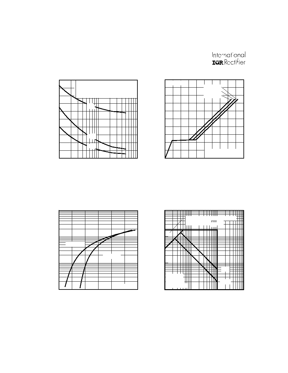
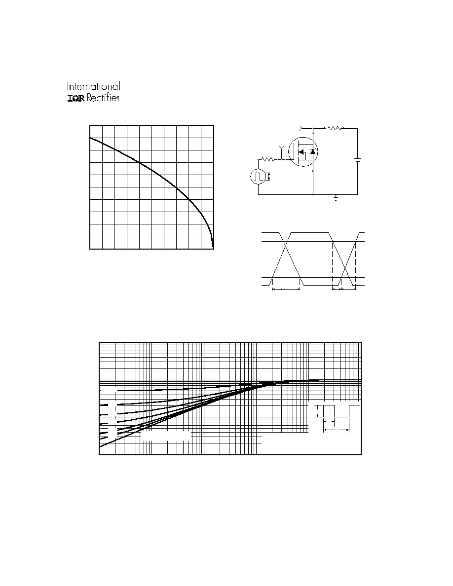
Fig 8. Maximum Safe Operating Area
Fig 6. Typical Gate Charge Vs.
Gate-to-Source Voltage
Fig 5. Typical Capacitance Vs.
Drain-to-Source Voltage
Fig 7. Typical Source-Drain Diode
Forward Voltage
1
10
100
0
1000
2000
3000
4000
5000
V , Drain-to-Source Voltage (V)
C, Capacitance (pF)
DS
V
C
C
C
=
=
=
=
0V,
C
C
C
f = 1MHz
+ C
+ C
C SHORTED
GS
iss
gs
gd ,
ds
rss
gd
oss
ds
gd
Ciss
Coss
Crss
0
40
80
120
160
200
0
4
8
12
16
20
Q , Total Gate Charge (nC)
V , Gate-to-Source Voltage (V)
G
GS
FOR TEST CIRCUIT
SEE FIGURE
I =
D
13
28A
V
= 20V
DS
V
= 50V
DS
V
= 80V
DS
1
10
100
1000
0.4
0.8
1.2
1.6
V ,Source-to-Drain Voltage (V)
I , Reverse Drain Current (A)
SD
SD
V = 0 V
GS
T = 25 C
J
°
T = 150 C
J
°
1
10
100
1000
VDS , Drain-toSource Voltage (V)
1
10
100
1000
I D
, Drain-to-Source Current (A)
Tc = 25°C
Tj = 150°C
Single Pulse
1ms
10ms
OPERATION IN THIS AREA
LIMITED BY R DS(on)
www.irf.com
5
IRF5N3710
Fig 10b. Switching Time Waveforms
Fig 11. Maximum Effective Transient Thermal Impedance, Junction-to-Case
Fig 9. Maximum Drain Current Vs.
Case Temperature
Fig 10a. Switching Time Test Circuit
V
DS
Pulse Width
1
µs
Duty Factor
0.1 %
R
D
V
GS
R
G
D.U.T.
+
-
V
DD
V
GS
V
DS
90%
10%
V
GS
t
d(on)
t
r
t
d(off)
t
f
0.01
0.1
1
10
0.00001
0.0001
0.001
0.01
0.1
1
Notes:
1. Duty factor D = t / t
2. Peak T = P
x Z
+ T
1
2
J
DM
thJC
C
P
t
t
DM
1
2
t , Rectangular Pulse Duration (sec)
Thermal Response
(Z )
1
thJC
0.01
0.02
0.05
0.10
0.20
D = 0.50
SINGLE PULSE
(THERMAL RESPONSE)
25
50
75
100
125
150
0
10
20
30
40
50
T , Case Temperature ( C)
I , Drain Current (A)
°
C
D