 | ÐлекÑÑоннÑй компоненÑ: IRF640S | СкаÑаÑÑ:  PDF PDF  ZIP ZIP |
Äîêóìåíòàöèÿ è îïèñàíèÿ www.docs.chipfind.ru
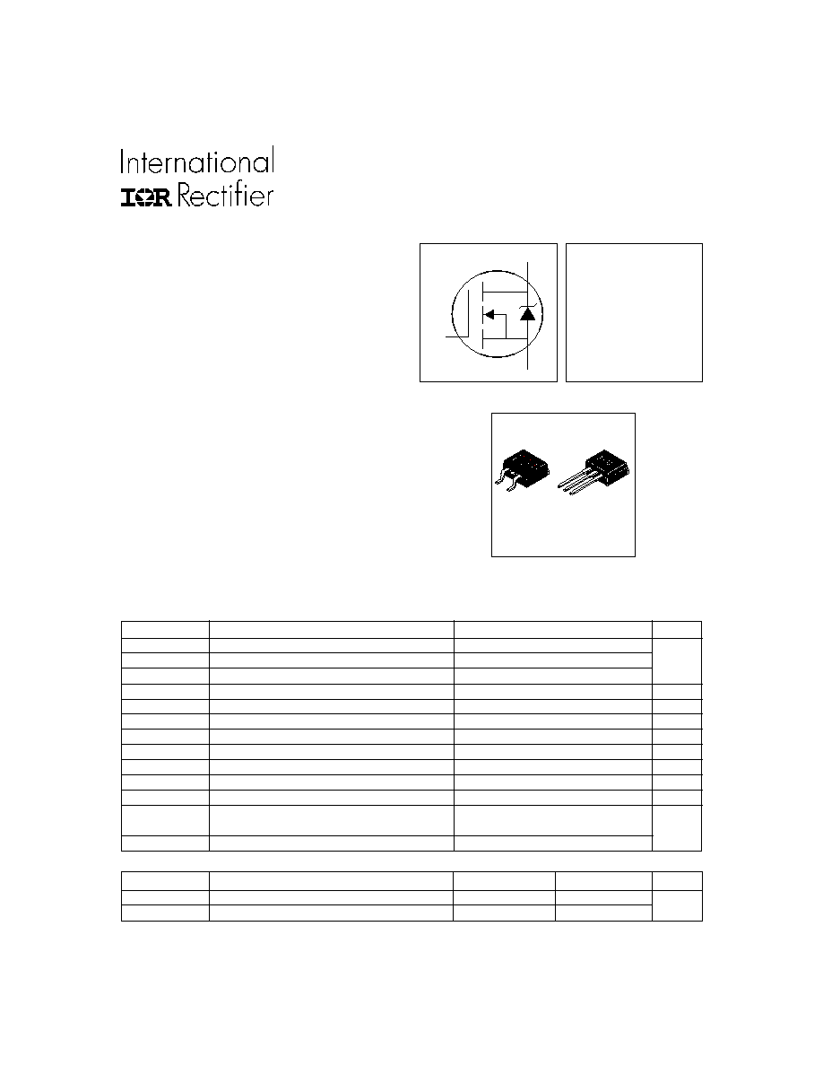
IRF640S/L
HEXFET
®
Power MOSFET
PD -90902B
S
D
G
Description
7/20/99
Parameter
Typ.
Max.
Units
R
JC
Junction-to-Case
1.0
R
JA
Junction-to-Ambient ( PCB Mounted,steady-state)**
40
Thermal Resistance
°C/W
Parameter
Max.
Units
I
D
@ T
C
= 25°C
Continuous Drain Current, V
GS
@ 10V
18
I
D
@ T
C
= 100°C
Continuous Drain Current, V
GS
@ 10V
11
A
I
DM
Pulsed Drain Current
72
P
D
@T
A
= 25°C
Power Dissipation
3.1
W
P
D
@T
C
= 25°C
Power Dissipation
130
W
Linear Derating Factor
1.0
W/°C
V
GS
Gate-to-Source Voltage
± 20
V
E
AS
Single Pulse Avalanche Energy
580
mJ
I
AR
Avalanche Current
18
A
E
AR
Repetitive Avalanche Energy
13
mJ
dv/dt
Peak Diode Recovery dv/dt
5.0
V/ns
T
J
Operating Junction and
-55 to + 175
T
STG
Storage Temperature Range
Soldering Temperature, for 10 seconds
300 (1.6mm from case )
°C
Absolute Maximum Ratings
l
Surface Mount (IRF640S)
l
Low-profile through-hole (IRF640L)
l
Available in Tape & Reel (IRF640S)
l
Dynamic dv/dt Rating
l
150°C Operating Temperature
l
Fast Switching
l
Fully Avalanche Rated
2
D P ak
T O -26 2
V
DSS
= 200V
R
DS(on)
= 0.18
I
D
= 18A
Third Generation HEXFETs from International Rectifier provide
the designer with the best combinations of fast switching ,
ruggedized device design, low on-resistance and cost-
effectiveness.
The D
2
Pak is a surface mount power package capable of
accommodating die sizes up to HEX-4. It provides the highest
power capability and the lowest possible on-resistance in any
existing surface mount package. The D
2
Pak is suitable for high
current applications because of its low internal connection
resistance and can dissipate up to 2.0W in a typical surface
mount application.The through-hole version (IRF640L) is
available for low-profile applications.
www.irf.com
1
IRF640S/L
2
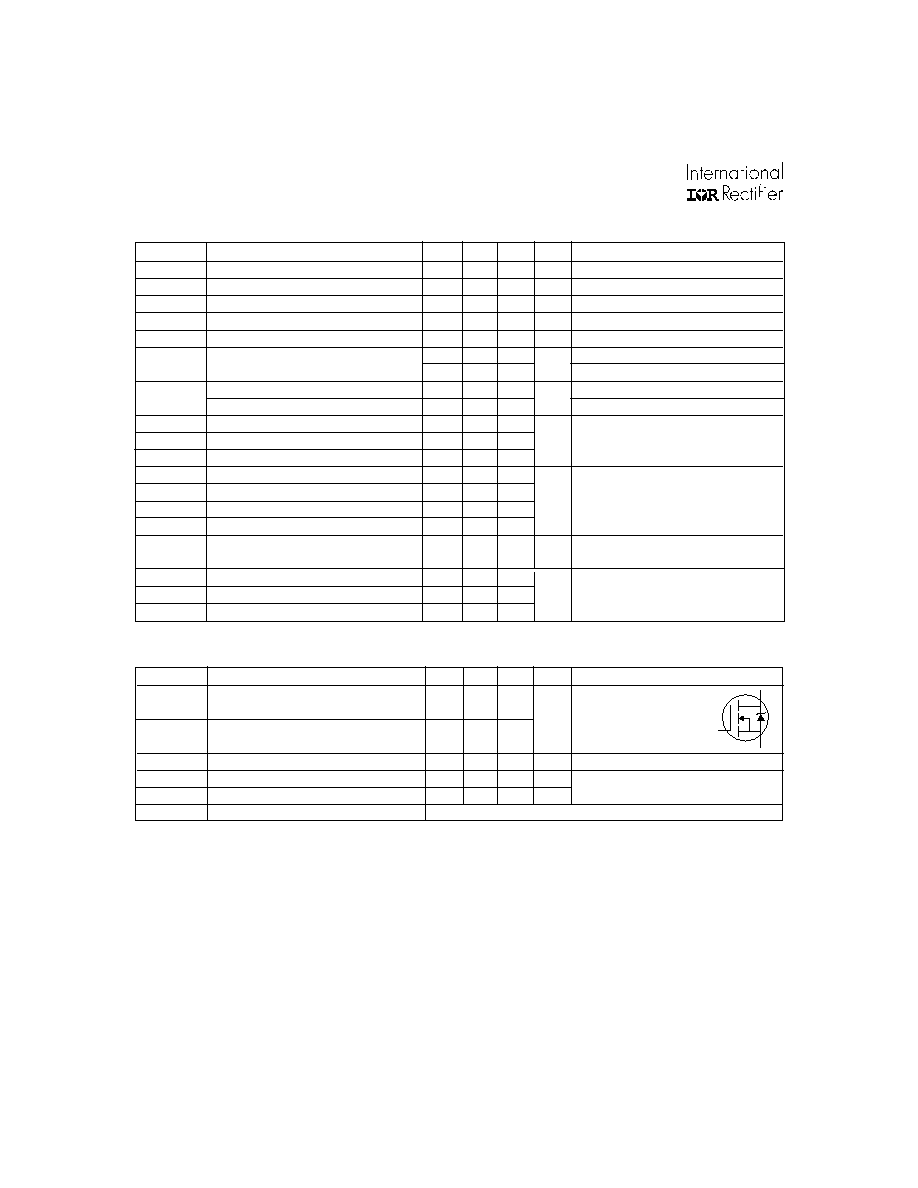
www.irf.com
Parameter
Min. Typ. Max. Units
Conditions
V
(BR)DSS
Drain-to-Source Breakdown Voltage
200
V
V
GS
= 0V, I
D
= 250µA
V
(BR)DSS
/
T
J
Breakdown Voltage Temp. Coefficient
0.29
V/°C
Reference to 25°C, I
D
= 1mA
R
DS(on)
Static Drain-to-Source On-Resistance
0.18
V
GS
= 10V, I
D
= 11A
V
GS(th)
Gate Threshold Voltage
2.0
4.0
V
V
DS
= V
GS
, I
D
= 250µA
g
fs
Forward Transconductance
6.7
S
V
DS
= 50V, I
D
= 11A
25
µ A
V
DS
= 200V, V
GS
= 0V
250
V
DS
= 160V, V
GS
= 0V, T
J
= 125°C
Gate-to-Source Forward Leakage
100
V
GS
= 20V
Gate-to-Source Reverse Leakage
-100
nA
V
GS
= -20V
Q
g
Total Gate Charge
70
I
D
= 18A
Q
gs
Gate-to-Source Charge
13
nC
V
DS
=160V
Q
gd
Gate-to-Drain ("Miller") Charge
39
V
GS
= 10V, See Fig. 6 and 13
t
d(on)
Turn-On Delay Time
14
V
DD
=100V
t
r
Rise Time
51
I
D
= 18A
t
d(off)
Turn-Off Delay Time
45
R
G
= 9.1
t
f
Fall Time
36
R
D
= 5.4
,
See Fig. 10
Between lead,
and center of die contact
C
iss
Input Capacitance
1300
V
GS
= 0V
C
oss
Output Capacitance
430
pF
V
DS
= 25V
C
rss
Reverse Transfer Capacitance
130
= 1.0MHz, See Fig. 5
Electrical Characteristics @ T
J
= 25°C (unless otherwise specified)
I
GSS
ns
I
DSS
Drain-to-Source Leakage Current
nH
7.5
L
S
Internal Source Inductance
V
DD
= 50V, starting T
J
= 25°C, L = 2.7mH
R
G
= 25
, I
AS
= 18A. (See Figure 12)
Repetitive rating; pulse width limited by
max. junction temperature. ( See fig. 11 )
Notes:
** When mounted on 1" square PCB ( FR-4 or G-10 Material ).
For recommended footprint and soldering techniques refer to application note #AN-994.
I
SD
18A, di/dt
150A/µs, V
DD
V
(BR)DSS
,
T
J
150°C
Pulse width
300µs; duty cycle
2%.
Uses IRF640 data and test conditions
Parameter
Min. Typ. Max. Units
Conditions
I
S
Continuous Source Current
MOSFET symbol
(Body Diode)
showing the
I
SM
Pulsed Source Current
integral reverse
(Body Diode)
p-n junction diode.
V
SD
Diode Forward Voltage
2.0
V
T
J
= 25°C, I
S
= 18A, V
GS
= 0V
t
rr
Reverse Recovery Time
300
610
ns
T
J
= 25°C, I
F
= 18A
Q
rr
Reverse Recovery Charge
3.4
7.1
µC
di/dt = 100A/µs
Source-Drain Ratings and Characteristics
S
D
G
A
18
72
t
on
Forward Turn-On Time
Intrinsic turn-on time is negligible (turn-on is dominated by L
S
+L
D
)
IRF640S/L
www.irf.com
3
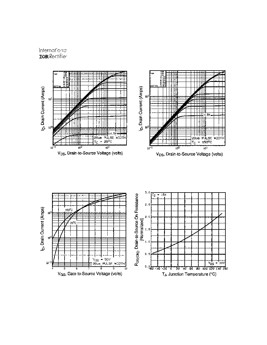
Fig 1. Typical Output Characteristics,
T
J
= 25
o
C
Fig 3. Typical Transfer Characteristics
Fig 4. Normalized On-Resistance
Vs. Temperature
Fig 2. Typical Output Characteristics,
T
J
= 175
o
C
IRF640S/L
4
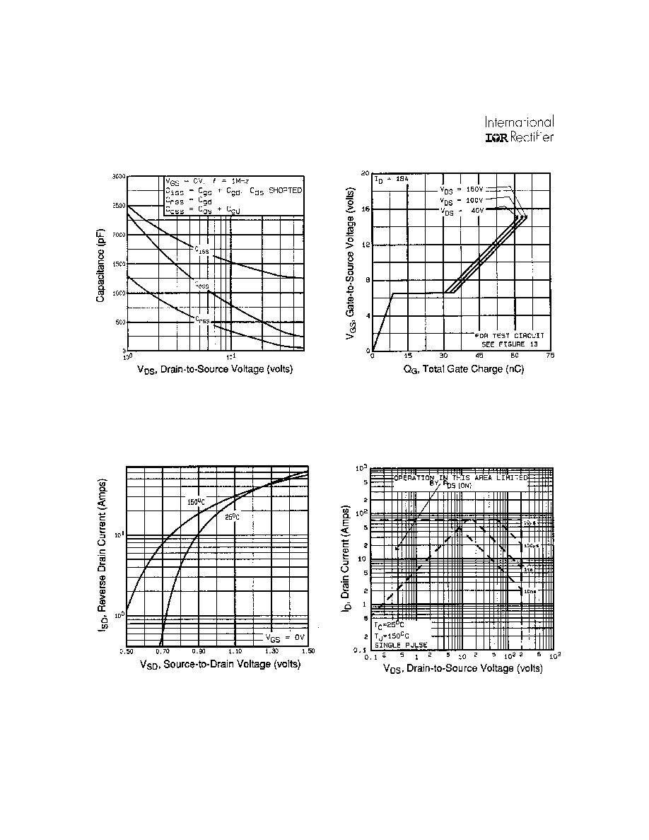
www.irf.com
Fig 7. Typical Source-Drain Diode
Forward Voltage
Fig 5. Typical Capacitance Vs.
Drain-to-Source Voltage
Fig 8. Maximum Safe Operating Area
Fig 6. Typical Gate Charge Vs.
Gate-to-Source Voltage
IRF640S/L
www.irf.com
5
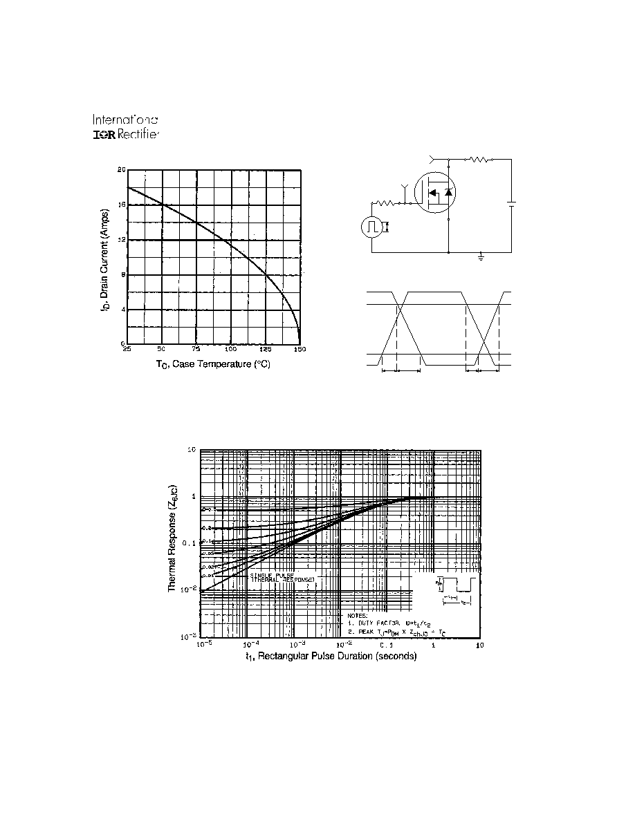
Fig 9. Maximum Drain Current Vs.
Case Temperature
Fig 10a. Switching Time Test Circuit
V
DS
90%
10%
V
GS
t
d(on)
t
r
t
d(off)
t
f
Fig 10b. Switching Time Waveforms
Fig 11. Maximum Effective Transient Thermal Impedance, Junction-to-Case
V
DS
Pulse Width
1
µs
Duty Factor
0.1 %
R
D
V
GS
R
G
D.U.T.
10V
+
-
V
DD