 | ÐлекÑÑоннÑй компоненÑ: IRF7805 | СкаÑаÑÑ:  PDF PDF  ZIP ZIP |
Äîêóìåíòàöèÿ è îïèñàíèÿ www.docs.chipfind.ru
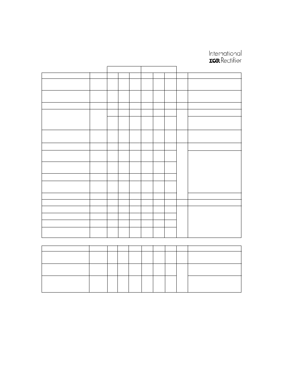
Parameter
Symbol
IRF7805
IRF7805A
Units
Drain-Source Voltage
V
DS
30
V
Gate-Source Voltage
V
GS
±12
Continuous Drain or Source
25°C
I
D
13
13
A
Current (V
GS
4.5V)
70°C
10
10
Pulsed Drain Current
I
DM
100
100
Power Dissipation
25°C
P
D
2.5
W
70°C
1.6
Junction & Storage Temperature Range
T
J
,
T
STG
55 to 150
°C
Continuous Source Current (Body Diode)
I
S
2.5
2.5
A
Pulsed source Current
I
SM
106
106
· N Channel Application Specific MOSFETs
· Ideal for Mobile DC-DC Converters
· Low Conduction Losses
· Low Switching Losses
Description
These new devices employ advanced HEXFET Power
MOSFET technology to achieve an unprecedented
balance of on-resistance and gate charge. The
reduced conduction and switching losses make them
ideal for high efficiency DC-DC Converters that power
the latest generation of mobile microprocessors.
The IRF7805/IRF7805A offers maximum efficiency for
mobile CPU core DC-DC converters.
HEXFET
®
Chip-Set for DC-DC Converters
IRF7805 IRF7805A
Vds
30V
30V
Rds(on) 11m
11m
Qg
31nC
31nC
Qsw
11.5nC
Qoss
36nC
36nC
Absolute Maximum Ratings
Parameter
Max.
Units
Maximum Junction-to-Ambient
R
JA
50
°C/W
Thermal Resistance
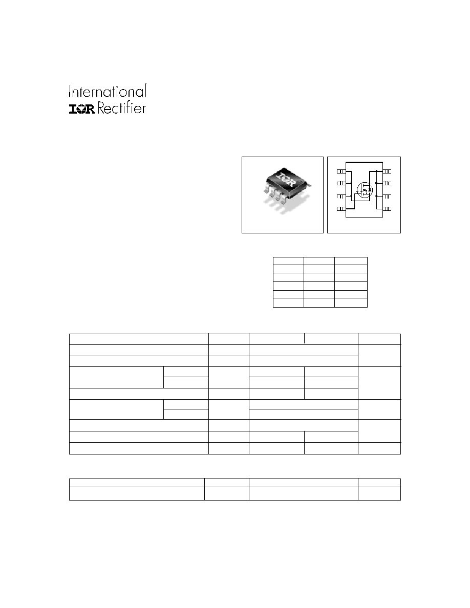
T o p V ie w
8
1
2
3
4
5
6
7
D
D
D
D
G
S
A
S
S
Device Features
IRF7805/IRF7805A
www.irf.com
1
10/10/00
SO-8
PD 91746C
www.irf.com
2
IRF7805/IRF7805A
Parameter
Min
Typ Max
Min
Typ Max Units
Conditions
Diode Forward
V
SD
1.2
1.2
V
I
S
= 7A
, V
GS
= 0V
Voltage*
Reverse Recovery
Q
rr
88
88
nC
di/dt = 700A/µs
Charge
V
DS
= 16V, V
GS
= 0V, I
S
= 7A
Reverse Recovery
Q
rr(s)
55
55
Charge (with Parallel
Schotkky)
Parameter
Min Typ Max
Min
Typ Max Units
Conditions
Drain-to-Source
V
(BR)DSS
30
30
V
V
GS
= 0V, I
D
= 250µA
Breakdown Voltage*
Static Drain-Source
R
DS
(on)
9.2
11
9.2
11
m
V
GS
= 4.5V, I
D
= 7A
on Resistance*
Gate Threshold Voltage* V
GS
(th)
1.0
1.0
V
V
DS
= V
GS
,I
D
= 250µA
Drain-Source Leakage
I
DSS
30
30
µA
V
DS
= 24V, V
GS
= 0
150
150
V
DS
= 24V, V
GS
= 0,
Tj = 100°C
Gate-Source Leakage
I
GSS
±100
±100
nA
V
GS
= ±12V
Current*
Total Gate Charge*
Q
g
22
31
22
31
V
GS
= 5V, I
D
= 7A
Pre-Vth
Q
gs1
3.7
3.7
V
DS
= 16V, I
D
= 7A
Gate-Source Charge
Post-Vth
Q
gs2
1.4
1.4
nC
Gate-Source Charge
Gate to Drain Charge
Q
gd
6.8
6.8
Switch Charge*
Q
SW
8.2
11.5
8.2
(Q
gs2
+ Q
gd
)
Output Charge*
Q
oss
30
36
30
36
V
DS
= 16V, V
GS
= 0
Gate Resistance
R
g
1.7
1.7
Turn-on Delay Time
t
d
(on)
16
16
V
DD
= 16V
Rise Time
t
r
20
20
ns
I
D
= 7A
Turn-off Delay Time
t
d
(off)
38
38
R
g
= 2
Fall Time
t
f
16
16
V
GS
= 4.5V
Resistive Load
Electrical Characteristics
Source-Drain Rating & Characteristics
Notes:
Repetitive rating; pulse width limited by max. junction temperature.
Pulse width
300 µs; duty cycle
2%.
When mounted on 1 inch square copper board, t < 10 sec.
Measured at V
DS
< 100mV. This approximates actual operation of a synchronous rectifier.
Typ = measured - Q
oss
*
Devices are 100% tested to these parameters.
IRF7805
IRF7805A
Current*
di/dt = 700A/µs
(with 10BQ040)
V
DS
= 16V, V
GS
= 0V, I
S
= 7A
www.irf.com
3
IRF7805/IRF7805A
Control FET
Special attention has been given to the power losses
in the switching elements of the circuit - Q1 and Q2.
Power losses in the high side switch Q1, also called the
Control FET, are impacted by the R
ds(on)
of the MOSFET,
but these conduction losses are only about one half of
the total losses.
Power losses in the control switch Q1 are given by;
P
loss
= P
conduction
+ P
switching
+ P
drive
+ P
output
This can be expanded and approximated by;
P
loss
=
I
rms
2
×
R
ds(on )
(
)
+
I
×
Q
gd
i
g
×
V
in
×
f
+
I
×
Q
gs2
i
g
×
V
in
×
f
+
Q
g
×
V
g
×
f
(
)
+
Q
oss
2
×
V
in
×
f
This simplified loss equation includes the terms Q
gs2
and Q
oss
which are new to Power MOSFET data sheets.
Q
gs2
is a sub element of traditional gate-source charge
that is included in all MOSFET data sheets. The impor-
tance of splitting this gate-source charge into two sub
elements, Q
gs1
and Q
gs2
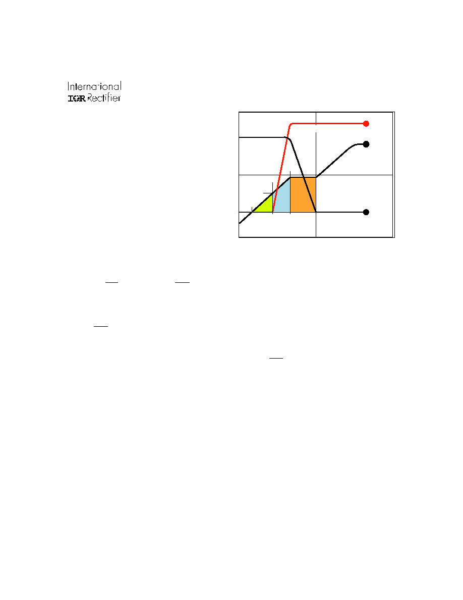
, can be seen from Fig 1.
Q
gs2
indicates the charge that must be supplied by
the gate driver between the time that the threshold volt-
age has been reached (t1) and the time the drain cur-
rent rises to I
dmax
(t2) at which time the drain voltage
begins to change. Minimizing Q
gs2
is a critical factor in
reducing switching losses in Q1.
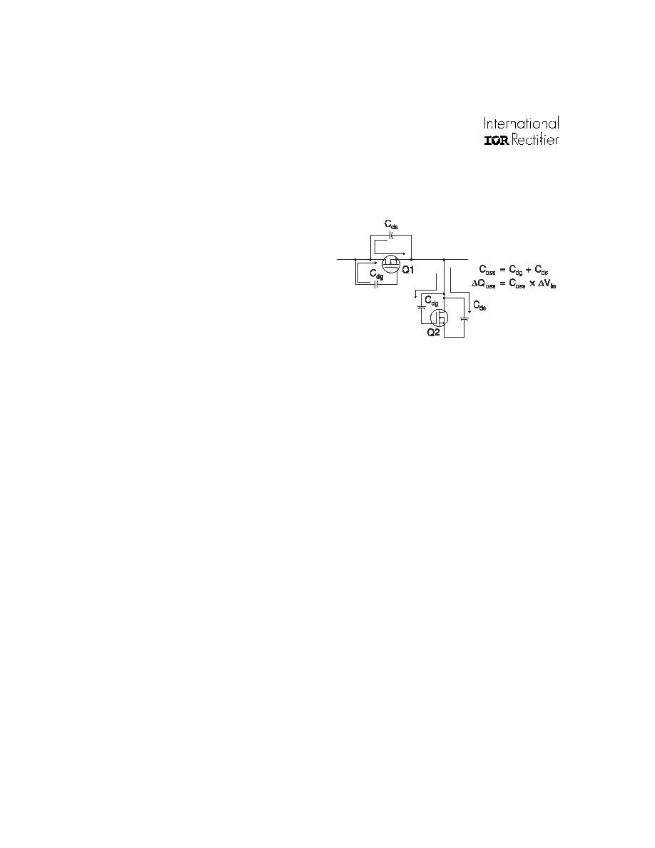
Q
oss
is the charge that must be supplied to the output
capacitance of the MOSFET during every switching
cycle. Figure 2 shows how Q
oss
is formed by the paral-
lel combination of the voltage dependant (non-linear)
capacitance's C
ds
and C
dg
when multiplied by the power
supply input buss voltage.
Figure 1: Typical MOSFET switching waveform
Synchronous FET
The power loss equation for Q2 is approximated
by;
P
loss
=
P
conduction
+
P
drive
+
P
output
*
P
loss
=
I
rms
2
×
R
ds(on)
(
)
+
Q
g
×
V
g
×
f
(
)
+
Q
oss
2
×
V
in
×
f
+
Q
rr
×
V
in
×
f
(
)
*dissipated primarily in Q1.
Power MOSFET Selection for DC/DC
Converters
4
1
2
Drain Current
Gate Voltage
Drain Voltage
t3
t2
t1
V
GTH
Q
GS1
Q
GS2
Q
GD
t0
www.irf.com
4
IRF7805/IRF7805A
Figure 2: Q
oss
Characteristic
For the synchronous MOSFET Q2, R
ds(on)
is an im-
portant characteristic; however, once again the impor-
tance of gate charge must not be overlooked since it
impacts three critical areas. Under light load the
MOSFET must still be turned on and off by the con-
trol IC so the gate drive losses become much more
significant. Secondly, the output charge Q
oss
and re-
verse recovery charge Q
rr
both generate losses that
are transfered to Q1 and increase the dissipation in
that device. Thirdly, gate charge will impact the
MOSFETs' susceptibility to Cdv/dt turn on.
The drain of Q2 is connected to the switching node
of the converter and therefore sees transitions be-
tween ground and V
in
. As Q1 turns on and off there is
a rate of change of drain voltage dV/dt which is ca-
pacitively coupled to the gate of Q2 and can induce
a voltage spike on the gate that is sufficient to turn
the MOSFET on, resulting in shoot-through current .
The ratio of Q
gd
/Q
gs1
must be minimized to reduce the
potential for Cdv/dt turn on.
Spice model for IRF7805 can be downloaded in ma-
chine readable format at www.irf.com.
www.irf.com
5
IRF7805/IRF7805A
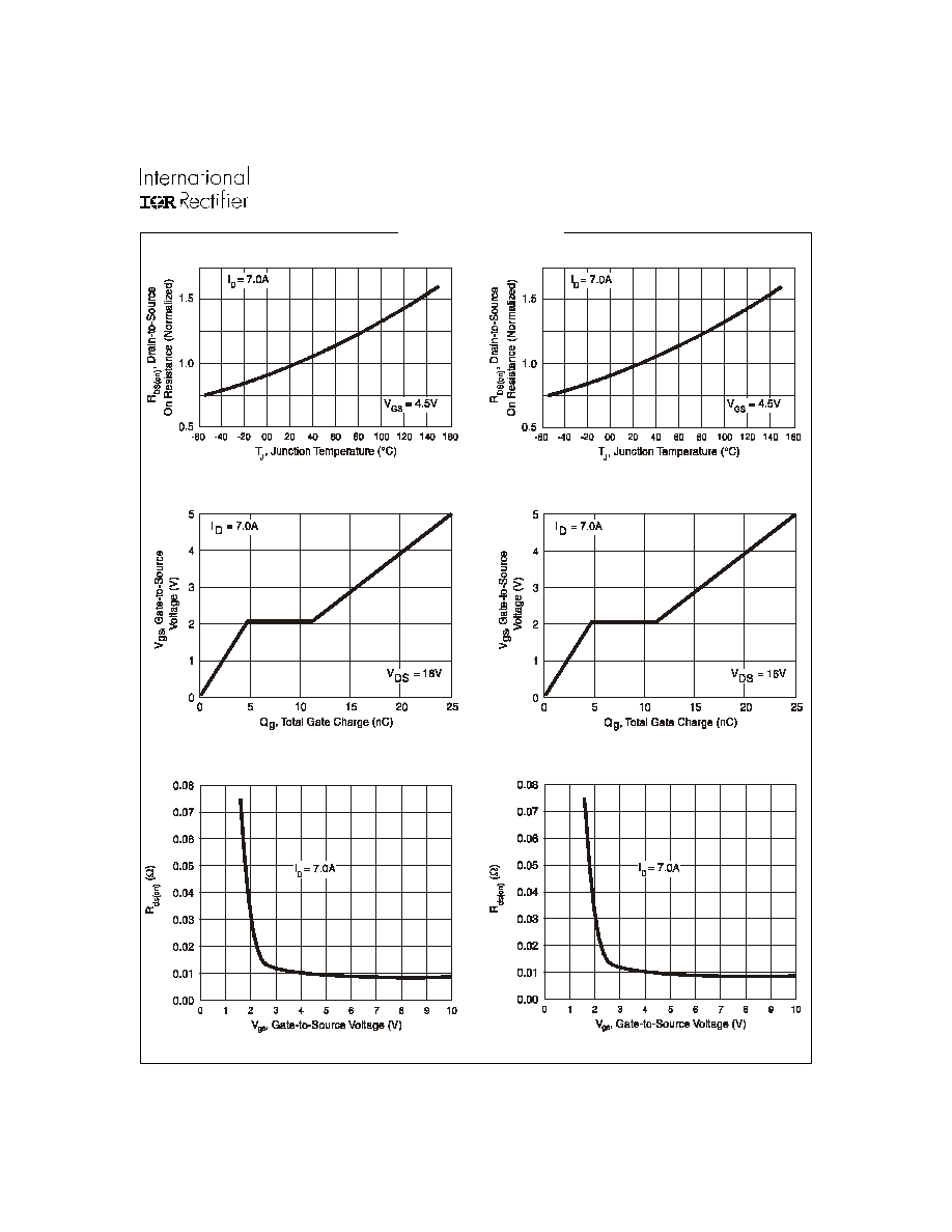
Figure 7. Typical Rds(on) vs. Gate-to-Source Voltage
Figure 5. Typical Gate Charge vs. Gate-to-Source Voltage
Figure 3. Normalized On-Resistance vs. Temperature
Figure 8. Typical Rds(on) vs. Gate-to-Source Voltage
Figure 6. Typical Gate Charge vs. Gate-to-Source Voltage
Figure 4. Normalized On-Resistance vs. Temperature
IRF7805
IRF7805A
Typical Characteristics