 | ÐлекÑÑоннÑй компоненÑ: IRF7811AV | СкаÑаÑÑ:  PDF PDF  ZIP ZIP |
Äîêóìåíòàöèÿ è îïèñàíèÿ www.docs.chipfind.ru
www.irf.com
1
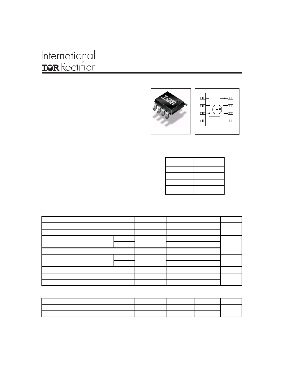
IRF7811AV
· N-Channel Application-Specific MOSFETs
· Ideal for CPU Core DC-DC Converters
· Low Conduction Losses
· Low Switching Losses
· Minimizes Parallel MOSFETs for high current
applications
· 100% R
G
Tested
Description
This new device employs advanced HEXFET Power
MOSFET technology to achieve an unprecedented
balance of on-resistance and gate charge. The reduced
conduction and switching losses make it ideal for high
efficiency DC-DC converters that power the latest
generation of microprocessors.
The IRF7811AV has been optimized for all parameters
that are critical in synchronous buck converters including
R
DS(on)
, gate charge and Cdv/dt-induced turn-on immunity.
The IRF7811AV offers an extremely low combination of
Q
sw
& R
DS(on)
for reduced losses in both control and
synchronous FET applications.
The package is designed for vapor phase, infra-red,
convection, or wave soldering techniques. Power
dissipation of greater than 2W is possible in a typical
PCB mount application.
DEVICE CHARACTERISTICS
Top View
8
1
2
3
4
5
6
7
D
D
D
D
G
S
A
S
S
A
IRF7811AV
SO-8
11/12/03
PD-94009A
IRF7811AV
R
DS(on)
11 m
Q
G
17 nC
Q
SW
6.7 nC
Q
OSS
8.1 nC
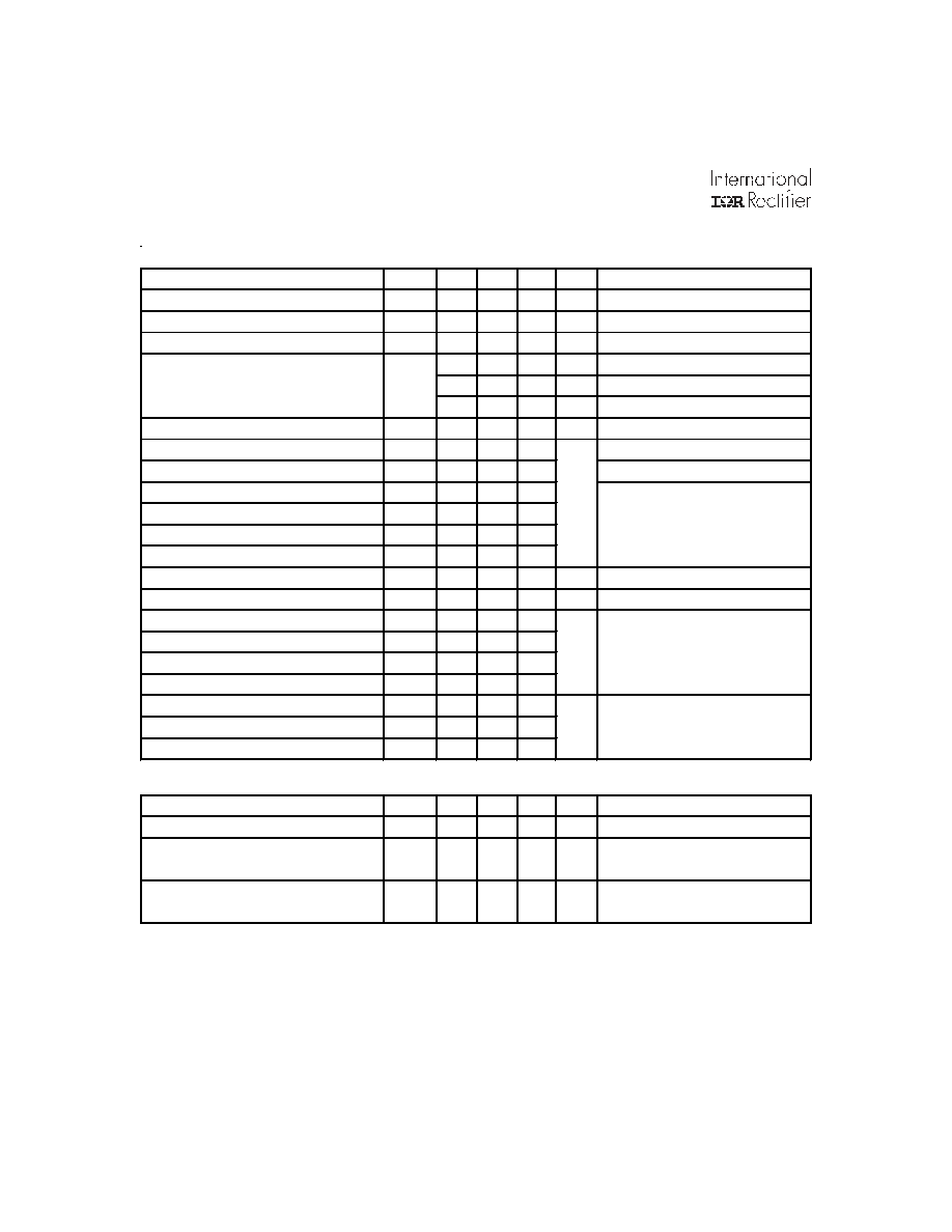
Absolute Maximum Ratings
Symbol
Units
V
DS
V
V
GS
Continuous Output Current T
A
= 25°C
A
(V
GS
4.5V)
T
L
= 90°C
I
DM
T
A
= 25°C
T
L
= 90°C
T
J
, T
STG
°C
I
S
I
SM
Thermal Resistance
Symbol
Typ
Max
Units
R
JA
50
R
JL
20
W
A
°C/W
Maximum Junction-to-Ambient
eh
Maximum Junction-to-Lead
hÃ
Pulsed Source Current
2.5
50
2.5
-55 to 150
I
D
P
D
Power Dissipation
eÃÃÃÃÃÃÃÃÃÃ
Continuous Source Current (Body Diode)
Parameter
Parameter
Drain-to-Source Voltage
Gate-to-Source Voltage
Pulsed Drain Current
Junction & Storage Temperature Range
3.0
IRF7811AV
10.8
100
30
±20
11.8
www.irf.com
2
IRF7811AV
Notes:
Repetitive rating; pulse width limited by max. junction temperature.
Pulse width
400 µs; duty cycle
2%.
When mounted on 1 inch square copper board, t < 10 sec.
Typ = measured - Q
oss
Typical values of R
DS
(on) measured at V
GS
= 4.5V, Q
G
, Q
SW
and Q
OSS
measured at V
GS
=5.0V, I
F
= 15A.
R
is measured at T
J
approximately 90°C
Electrical Characteristics
Parameter
Symbol Min
Typ
Max Units
Drain-to-Source Breakdown Voltage
V
(BR)DSS
30
V
Static Drain-to-Source On-Resistance
R
DS(on)
11
14
m
Gate Threshold Voltage
V
GS(th)
1.0
3.0
V
50
µA
20
µA
100
mA
Gate-to-Source Leakage Current
I
GSS
±100
nA
Total Gate Charge, Control FET
Q
g
17
26
nC
Total Gate Charge, Synch FET
Q
g
14
21
V
GS
= 5.0V, V
DS
< 100mV
Pre-Vth Gate-to-Source Charge
Q
gs1
3.4
Post-Vth Gate-to-Source Charge
Q
gs2
1.6
Gate-to-Drain ("Miller") Charge
Q
gd
5.1
Switch Charge (Q
gs2
+ Q
gd
)
Q
SW
6.7
Output Charge
Q
OSS
8.1
12
V
DS
= 16V, V
GS
= 0
Gate Resistance
R
G
0.5
4.4
Turn-On Delay Time
t
d(on)
8.6
ns
Rise Time
t
r
21
Turn-Off Delay Time
t
d(off)
43
Fall Time
t
f
10
Input Capacitance
C
iss
1801
pF
Output Capacitance
C
oss
723
Reverse Transfer Capacitance
C
rss
46
Diode Characteristics
Parameter
Symbol Min
Typ
Max Units
Diode Forward Voltage
V
SD
1.3
V
Reverse Recovery Charge
(with Parallel Schottsky)
f
V
DS
= V
GS
, I
D
= 250µA
V
DS
= 30V, V
GS
= 0V
V
GS
= ± 20V
V
DS
= 24V, I
D
= 15A, V
GS
= 5.0V
V
DS
= 24V, V
GS
= 0V
Conditions
V
GS
= 0V, I
D
= 250µA
V
GS
= 4.5V, I
D
= 15A
d
di/dt = 700A/µs , (with 10BQ040)
V
DD
= 16V, V
GS
= 0V, I
D
= 15A
V
GS
= 5.0V
V
DD
= 16V
I
D
= 15A
Clamped Inductive Load
di/dt = 700A/µs
V
DD
= 16V, V
GS
= 0V, I
D
= 15A
T
J
= 25°C, I
S
= 15A
d
,V
GS
= 0V
V
DS
= 24V, V
GS
= 0V, T
J
= 100°C
V
GS
= 0V
V
DS
= 10V
Conditions
Drain-to-Source Leakage Current
I
DSS
V
DS
= 16V, I
D
= 15A
Q
rr
43
nC
nC
50
Q
rr
Reverse Recovery Charge
f
www.irf.com
3
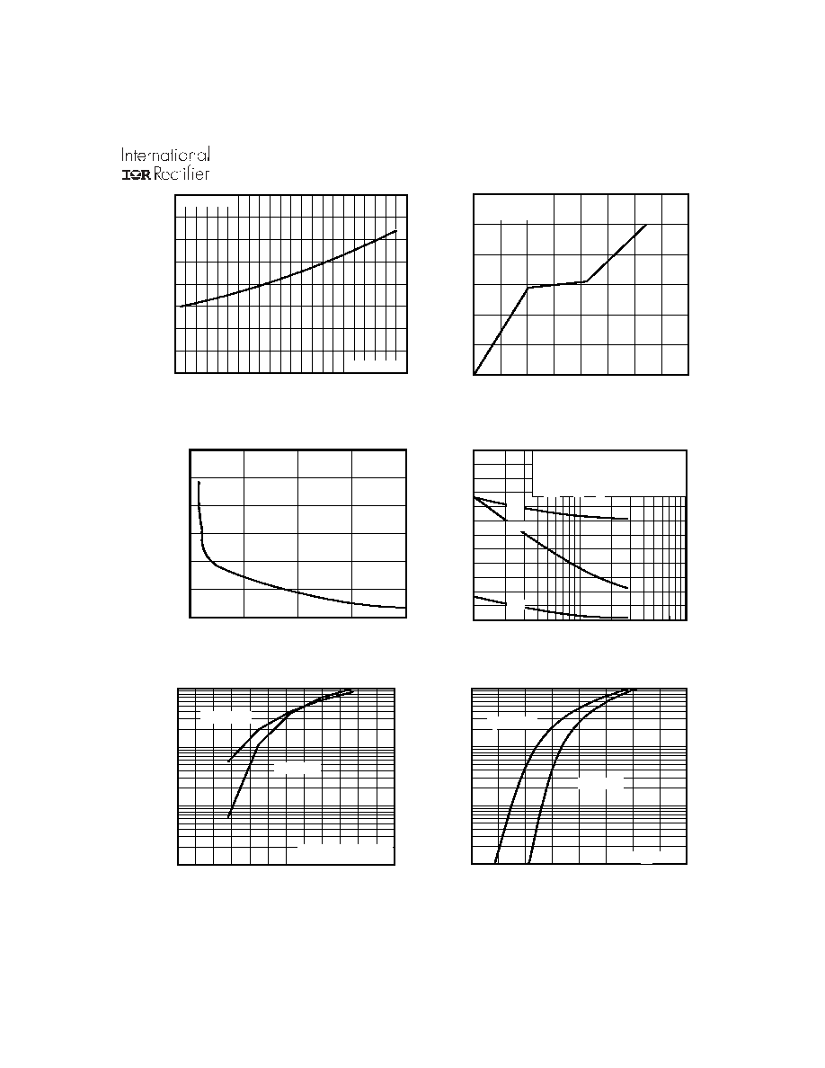
IRF7811AV
0
5
10
15
20
0
2
4
6
Q , Total Gate Charge (nC)
V
,
G
a
t
e
-
t
o-
S
our
c
e
V
o
lt
age (
V
)
G
GS
I
=
D
15A
1
10
100
V DS , Drain-to-Source Voltage (V)
0
500
1000
1500
2000
2500
3000
C
,
C
a
p
a
c
i
t
a
n
c
e
(
p
F
)
Coss
Crss
Ciss
V GS = 0V, f = 1 MHZ
Ciss = Cgs + Cgd , Cds SHORTED
Crss = Cgd
Coss = Cds + Cgd
0.1
1
10
100
2.0
2.5
3.0
3.5
4.0
4.5
5.0
V = 15V
20µs PULSE WIDTH
DS
V , Gate-to-Source Voltage (V)
I , Dr
a
i
n
-
to
-
S
o
u
r
ce
Cu
r
r
e
n
t
(
A
)
GS
D
T = 25 C
J
°
T = 150 C
J
°
0.1
1
10
100
0.3
0.6
0.9
1.2
1.5
V ,Source-to-Drain Voltage (V)
I , R
e
verse D
r
ai
n C
u
rrent (A
)
SD
SD
V = 0 V
GS
T = 25 C
J
°
T = 150 C
J
°
Figure 1. Normalized On-Resistance vs. Temperature
Figure 2. Gate-to-Source Voltage vs. Typical Gate Charge
Figure 3. Typical Rds(on) vs. Gate-to-Source Voltage
Figure 4. Typical Capacitance vs. Drain-to-Source Voltage
Figure 5. Typical Transfer Characteristics
Figure 6. Typical Source-Drain Diode Forward Voltage
-60
-40
-20
0
20
40
60
80
100
120
140
160
0.0
0.5
1.0
1.5
2.0
T , Junction Temperature
( C)
R
, D
r
a
i
n
-
to
-
S
o
u
r
c
e
O
n
R
e
s
i
s
t
a
n
c
e
(Norm
a
liz
ed)
J
DS(on)
°
V
=
I
=
GS
D
4.5V
15A
V
DS
= 16V
3.0
6.0
9.0
12.0
15.0
V GS, Gate -to -Source Voltage (V)
0.008
0.010
0.012
0.014
0.016
0.018
0.020
R
D
S
(
o
n
)
,
D
r
a
i
n
-
t
o
-
S
o
u
r
c
e
O
n
R
e
s
i
s
t
a
n
c
e
(
)
ID = 15A
www.irf.com
4
IRF7811AV
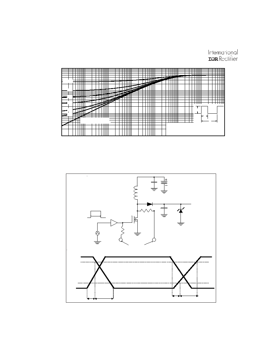
Figure 7. Maximum Effective Transient Thermal Impedance, Junction-to-Ambient
0.1
1
10
100
0.0001
0.001
0.01
0.1
1
10
100
1000
Notes:
1. Duty factor D = t / t
2. Peak T = P
x Z
+ T
1
2
J
DM
thJA
A
P
t
t
DM
1
2
t , Rectangular Pulse Duration (sec)
Thermal R
e
sponse
(Z )
1
th
JA
0.01
0.02
0.05
0.10
0.20
D = 0.50
SINGLE PULSE
(THERMAL RESPONSE)
Figure 8. Clamped Inductive load test diagram and switching waveform
50 Ohms probe
125 nS
50 u
5 uH
Scho ttky -6A
VDD
16Vz500mW
50 u
450
450
Mic4452 BM
Rep etition rate:100Hz
8V
Switching Time Waveforms
10%
90%
V
ds
V
gs
t
d(on)
t
f(v)
t
d(off)
t
r
(v)
www.irf.com
5
IRF7811AV
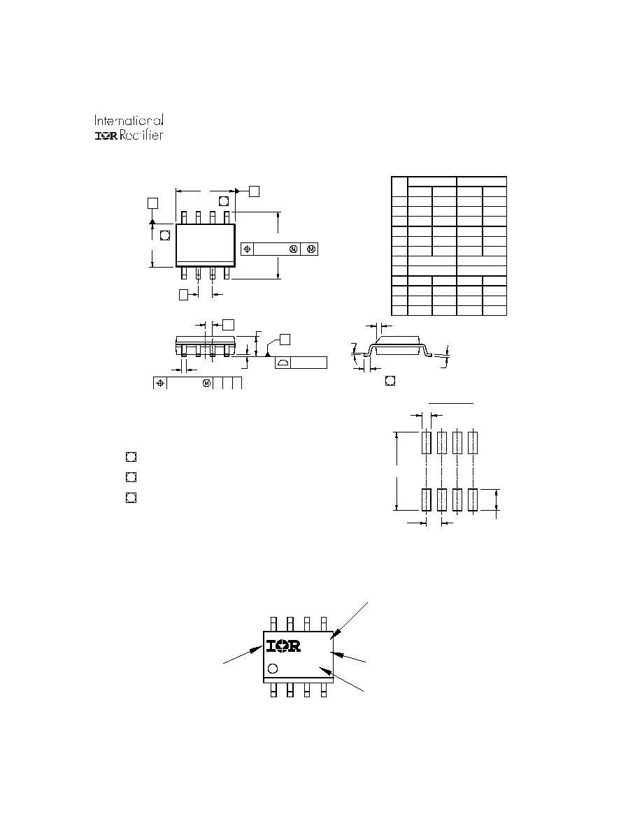
SO-8 Package Details
SO-8 Part Marking
e 1
D
E
y
b
A
A1
H
K
L
.189
.1497
0°
.013
.050 BASIC
.0532
.0040
.2284
.0099
.016
.1968
.1574
8°
.020
.0688
.0098
.2440
.0196
.050
4.80
3.80
0.33
1.35
0.10
5.80
0.25
0.40
0°
1.27 BASIC
5.00
4.00
0.51
1.75
0.25
6.20
0.50
1.27
MIN
MAX
MILLIMETERS
INCHES
MIN
MAX
DIM
8°
e
c
.0075
.0098
0.19
0.25
.025 BASIC
0.635 BASIC
8
7
5
6
5
D
B
E
A
e
6X
H
0.25 [.010]
A
6
7
K x 45°
8X L
8X c
y
0.25 [.010]
C A B
e1
A
A1
8X b
C
0.10 [.004]
4
3
1
2
FOOTPRINT
8X 0.72 [.028]
6.46 [.255]
3X 1.27 [.050]
4. OUTLINE CONFORMS TO JEDEC OUTLINE MS-012AA.
NOTES:
1. DIMENSIONING & TOLERANCING PER ASME Y14.5M-1994.
2. CONTROLLING DIMENSION: MILLIMETER
3. DIMENSIONS ARE SHOWN IN MILLIMETERS [INCHES].
5 DIMENSION DOES NOT INCLUDE MOLD PROTRUSIONS.
6 DIMENSION DOES NOT INCLUDE MOLD PROTRUSIONS.
MOLD PROTRUSIONS NOT TO EXCEED 0.25 [.010].
7 DIMENSION IS THE LENGTH OF LEAD FOR SOLDERING TO
A SUBSTRATE.
MOLD PROTRUSIONS NOT TO EXCEED 0.15 [.006].
8X 1.78 [.070]
EXAMPLE: THIS IS AN IRF7101 (MOSFET)
INTERNATIONAL
RECTIFIER
LOGO
F7101
YWW
XXXX
PART NUMBER
LOT CODE
WW = WEEK
Y = LAST DIGIT OF THE YEAR
DATE CODE (YWW)