 | ÐлекÑÑоннÑй компоненÑ: IRF7822 | СкаÑаÑÑ:  PDF PDF  ZIP ZIP |
Äîêóìåíòàöèÿ è îïèñàíèÿ www.docs.chipfind.ru
Parameter
Symbol
IRF7822
Units
Drain-Source Voltage
V
DS
30
V
Gate-Source Voltage
V
GS
±12
Continuous Drain or Source
T
A
= 25°C
I
D
18
Current (V
GS
4.5V)
T
A
= 70°C
13
A
Pulsed Drain Current
Q
I
DM
150
Power Dissipation
T
A
= 25°C
P
D
3.1
W
T
A
= 70°C
3.0
Junction & Storage Temperature Range
T
J
,
T
STG
55 to 150
°C
Continuous Source Current (Body Diode)
I
S
3.8
A
Pulsed Source Current
Q
I
SM
150
Absolute Maximum Ratings
Parameter
Max.
Units
Maximum Junction-to-Ambient
S
R
JA
40
°C/W
Maximum Junction-to-Lead
R
JL
20
°C/W
Thermal Resistance
IRF7822
07/11/01
IRF7822
R
DS
(on)
5.0m
Q
G
44nC
Q
sw
12nC
Q
oss
27nC
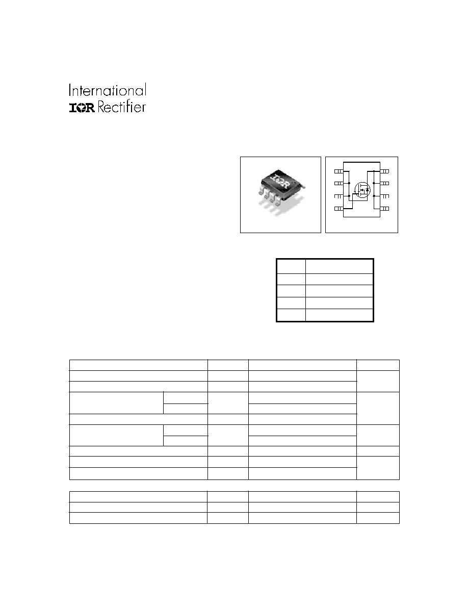
DEVICE CHARACTERISTICS
U
T o p V ie w
8
1
2
3
4
5
6
7
D
D
D
D
G
S
A
S
S
SO-8
HEXFET
®
Power MOSFET for DC-DC Converters
· N-Channel Application-Specific MOSFETs
· Ideal for CPU Core DC-DC Converters
· Low Conduction Losses
· Low Switching Losses
Description
This new device employs advanced HEXFET Power
MOSFET technology to achieve an unprecedented
balance of on-resistance and gate charge. The reduced
conduction and switching losses make it ideal for high
efficiency DC-DC converters that power the latest
generation of microprocessors.
The IRF7822 has been optimized for all parameters that
are critical in synchronous buck converters including
R
DS(on)
, gate charge and Cdv/dt-induced turn-on immunity.
The IRF7822 offers particulary low R
DS(on)
and high Cdv/
dt immunity for synchronous FET applications.
The package is designed for vapor phase, infra-red,
convection, or wave soldering techniques. Power
dissipation of greater than 3W is possible in a typical
PCB mount application.
www.irf.com
1
PD - 94279
IRF7822
2
www.irf.com
Parameter
Min
Typ
Max
Units
Conditions
Diode Forward
V
SD
1.0
V
I
S
= 15A
R
, V
GS
= 0V
Voltage*
Reverse Recovery
Q
rr
120
nC
di/dt
~
700A/µs
V
DS
= 16V, V
GS
= 0V, I
S
= 15A
Reverse Recovery
Q
rr(s)
108
nC
di/dt = 700A/µs
Charge (with Parallel
(with 10BQ040)
Schottky)
T
V
DS
= 16V, V
GS
= 0V, I
S
= 15A
Source-Drain Rating & Characteristics
Charge
T
Notes:
Q
Repetitive rating; pulse width limited by max. junction temperature.
R
Pulse width
400 µs; duty cycle
2%.
S
When mounted on 1 inch square copper board
T
Typ = measured - Q
oss
U
Typical values of R
DS
(on) measured at V
GS
= 4.5V, Q
G
, Q
SW
and Q
OSS
measured at V
GS
= 5.0V, I
F
= 15A.
Parameter
Min
Typ
Max
Units
Conditions
Drain-to-Source
BV
DSS
30
V
V
GS
= 0V, I
D
= 250µA
Breakdown Voltage
Static Drain-Source
R
DS(on)
5.0
6.5
m
V
GS
= 4.5V, I
D
= 15A
R
on Resistance
Gate Threshold Voltage
V
GS(th)
1.0
V
V
DS
= V
GS
,I
D
= 250µA
Drain-Source Leakage
I
DSS
30
V
DS
= 24V, V
GS
= 0
Current*
150
µA
V
DS
= 24V, V
GS
= 0,
Tj = 100°C
Gate-Source Leakage
I
GSS
±100
nA
V
GS
= ±12V
Current
Total Gate Chg Cont FET
Q
G
44
60
V
GS
=5.0V, I
D
=15A, V
DS
=16V
Total Gate Chg Sync FET
Q
G
38
V
GS
= 5.0V, V
DS
< 100mV
Pre-Vth
Q
GS1
13
V
DS
= 16V, I
D
= 15A
Gate-Source Charge
Post-Vth
Q
GS2
3.0
nC
Gate-Source Charge
Gate to Drain Charge
Q
GD
9.0
Switch Chg(Q
gs2
+ Q
gd
)
Q
sw
12
Output Charge
Q
oss
27
V
DS
= 16V, V
GS
= 0
Gate Resistance
R
G
1.5
Turn-on Delay Time
t
d (on)
15
V
DD
= 16V, I
D
= 15A
Rise Time
t
r
5.5
ns V
GS
= 5.0V
Turn-off Delay Time
t
d
(off)
22
Clamped Inductive Load
Fall Time
t
f
12
Input Capacitance
C
iss
5500
Output Capacitance
C
oss
1000
pF
V
DS
= 16V, V
GS
= 0
Reverse Transfer Capacitance C
rss
300
Electrical Characteristics
Current
IRF7822
www.irf.com
3
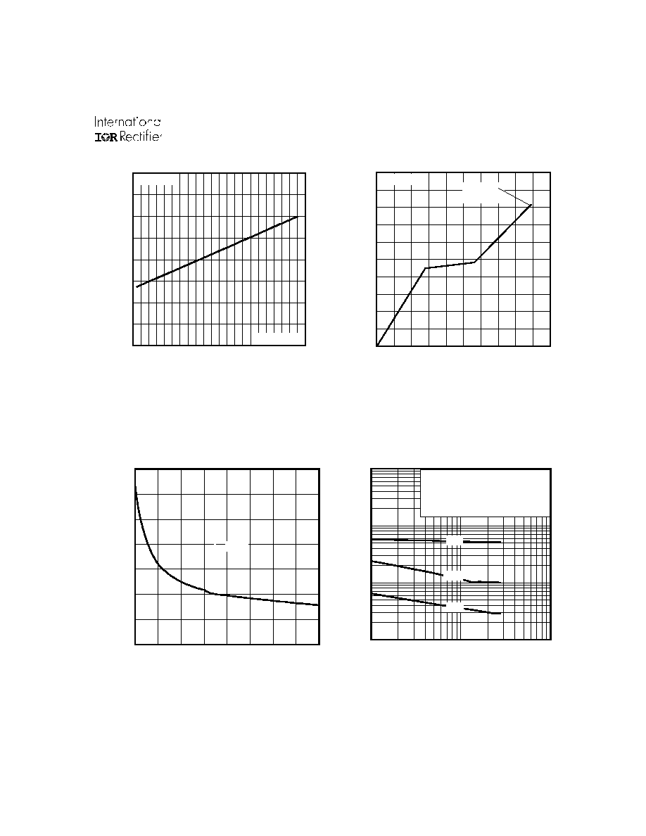
Fig 1. Normalized On-Resistance
Vs. Temperature
Fig 2. Typical Gate Charge Vs.
Gate-to-Source Voltage
Fig 3. On-Resistance Vs. Gate Voltage
Fig 4. Typical Capacitance Vs.
Drain-to-Source Voltage
-60 -40 -20
0
20
40
60
80 100 120 140 160
0.0
0.5
1.0
1.5
2.0
T , Junction Temperature ( C)
R , Drain-to-Source On Resistance
(Normalized)
J
DS(on)
°
V
=
I =
GS
D
4.5V
15A
3.0
4.0
5.0
6.0
7.0
VGS, Gate -to -Source Voltage (V)
0.003
0.004
0.005
0.006
0.007
0.008
0.009
0.010
R
DS(on)
, Drain-to -Source On Resistance (
)
ID = 15A
1
10
100
VDS, Drain-to-Source Voltage (V)
100
1000
10000
100000
C, Capacitance(pF)
Coss
Crss
Ciss
VGS = 0V, f = 1 MHZ
Ciss = Cgs + Cgd, Cds SHORTED
Crss = Cgd
Coss = Cds + Cgd
0
10
20
30
40
50
0
1
2
4
5
6
Q , Total Gate Charge (nC)
V , Gate-to-Source Voltage (V)
G
GS
I
=
D
15A
V
= 24V
DS
IRF7822
4
www.irf.com
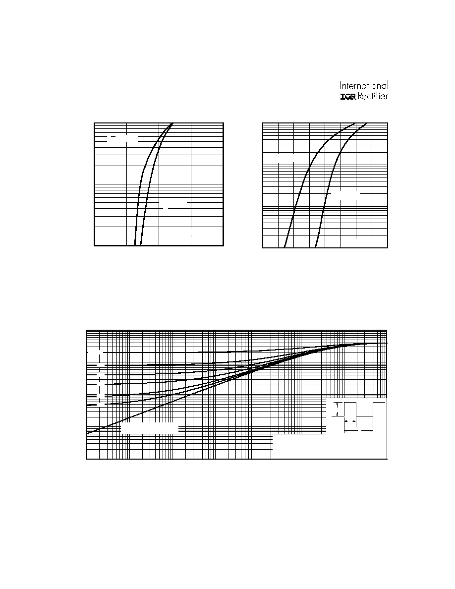
Figure 7. Maximum Effective Transient Thermal Impedance, Junction-to-Ambient
Fig 6. Typical Source-Drain Diode
Forward Voltage
Fig 5. Typical Transfer Characteristics
0.1
1
10
100
0.2
0.5
0.7
1.0
1.2
V ,Source-to-Drain Voltage (V)
I , Reverse Drain Current (A)
SD
SD
V = 0 V
GS
T = 150 C
J
°
T = 25 C
J
°
1.0
2.0
3.0
4.0
5.0
VGS, Gate-to-Source Voltage (V)
1.00
10.00
100.00
I D
, Drain-to-Source Current
(
)
TJ = 25°C
TJ = 175°C
VDS = 15V
20µs PULSE WIDTH
0.01
0.1
1
10
100
0.00001
0.0001
0.001
0.01
0.1
1
10
100
Notes:
1. Duty factor D =
t / t
2. Peak T
= P
x Z
+ T
1
2
J
DM
thJA
A
P
t
t
DM
1
2
t , Rectangular Pulse Duration (sec)
Thermal Response
(Z )
1
thJA
0.01
0.02
0.05
0.10
0.20
D = 0.50
SINGLE PULSE
(THERMAL RESPONSE)
IRF7822
www.irf.com
5
SO-8 Package Details
K x 45 °
C
8X
L
8 X
H
0.2 5 (.0 10 ) M A M
A
0 .10 (.00 4)
B 8X
0 .25 (.01 0) M C A S B S
- C -
6X
e
- B -
D
E
- A -
8 7 6 5
1 2 3 4
5
6
5
R E CO M M E ND E D F O O TP R IN T
0 .72 (.02 8 )
8 X
1 .78 (.07 0)
8X
6 .46 ( .25 5 )
1.27 ( .0 50 )
3X
D IM
IN C H E S M IL LIM E T E R S
M IN M A X M IN M A X
A .0532 .0688 1 .35 1 .75
A 1 .0040 .0098 0 .10 0 .25
B .014 .018 0 .36 0 .46
C .0 075 .0 098 0 .19 0.25
D .1 89 .1 96 4 .80 4.98
E .150 .157 3 .81 3 .99
e .050 B A S IC 1.2 7 B A S IC
e1 .025 B A S IC 0.6 35 B A S IC
H .2 284 .2 440 5 .80 6.20
K .011 .019 0 .28 0 .48
L 0 .16 .050 0 .41 1.27
0° 8° 0 ° 8°
N O TE S :
1 . D IM EN SIO N IN G AN D TO L ER A NC IN G P ER AN S I Y1 4.5 M -198 2.
2 . C O N T RO L LIN G D IM EN SIO N : IN C H .
3 . D IM EN SIO N S A RE SH O W N IN M ILLIM E TE R S (IN C HE S).
4 . O U T LIN E CO N F O RM S T O JED E C O U T LINE M S -0 12 AA .
D IM E NS IO N D O ES N O T IN C LU D E M O LD PR O T R US IO N S
M O LD P R O TR U SIO NS N O T T O EXCE ED 0 .2 5 (.00 6).
D IM E NS IO N S IS T H E LE N G TH O F L EA D F O R SO L DE R IN G TO A SU B ST RA T E..
5
6
A 1
e 1
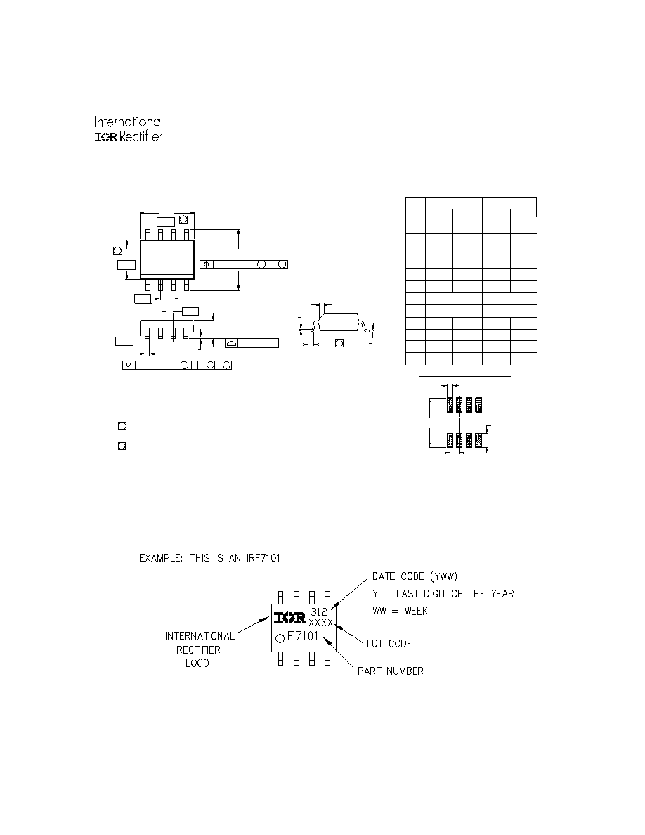
SO-8 Part Marking