 | ÐлекÑÑоннÑй компоненÑ: IRF840LCL | СкаÑаÑÑ:  PDF PDF  ZIP ZIP |
Äîêóìåíòàöèÿ è îïèñàíèÿ www.docs.chipfind.ru
HEXFET
®
Power MOSFET
PD- 93766
This new series of low charge HEXFET
®
power MOSFETs
achieve significant lower gate charge over conventional
MOSFETs. Utilizing the new LCDMOS (low charge
device MOSFETs) technology, the device improvements
are achieved without added product cost, allowing for
reduce gate drive requirements and total system savings.
In addition, reduced switching losses and improved
efficiency and achievable in a variety of high frequency
applications. Frequencies of a few MHz at high current
are possible using the new low charge MOSFETs.
These device improvements combined with the proven
ruggedness and reliability that characterize of HEXFET
power MOSFETs offer the designer a new power
transistor standard for switching applications.
S
D
G
V
DSS
= 500V
R
DS(on)
= 0.85
I
D
= 8.0A
l
Ultra Low Gate Charge
l
Reduced Gate Drive Requirement
l
Enhanced 30V V
GS
Rating
l
Reduced C
ISS
, C
OSS
, C
RSS
l
Extremely High Frequency Operation
l
Repetitive Avalanche Rated
Description
1/3/2000
Parameter
Typ.
Max.
Units
R
JC
Junction-to-Case
1.0
R
JA
Junction-to-Ambient (PCB Mounted,steady-state)**
40
Thermal Resistance
°C/W
Parameter
Max.
Units
I
D
@ T
C
= 25°C
Continuous Drain Current, V
GS
@ 10V
8.0
I
D
@ T
C
= 100°C
Continuous Drain Current, V
GS
@ 10V
5.1
A
I
DM
Pulsed Drain Current
28
P
D
@T
A
= 25°C
Power Dissipation
3.1
W
P
D
@T
C
= 25°C
Power Dissipation
125
W
Linear Derating Factor
1.0
W/°C
V
GS
Gate-to-Source Voltage
± 30
V
E
AS
Single Pulse Avalanche Energy,
510
mJ
I
AR
Avalanche Current
8.0
A
E
AR
Repetitive Avalanche Energy
13
mJ
dv/dt
Peak Diode Recovery dv/dt
3.5
V/ns
T
J
Operating Junction and
-55 to + 150
T
STG
Storage Temperature Range
Soldering Temperature, for 10 seconds
300 (1.6mm from case)
°C
Absolute Maximum Ratings
www.irf.com
1
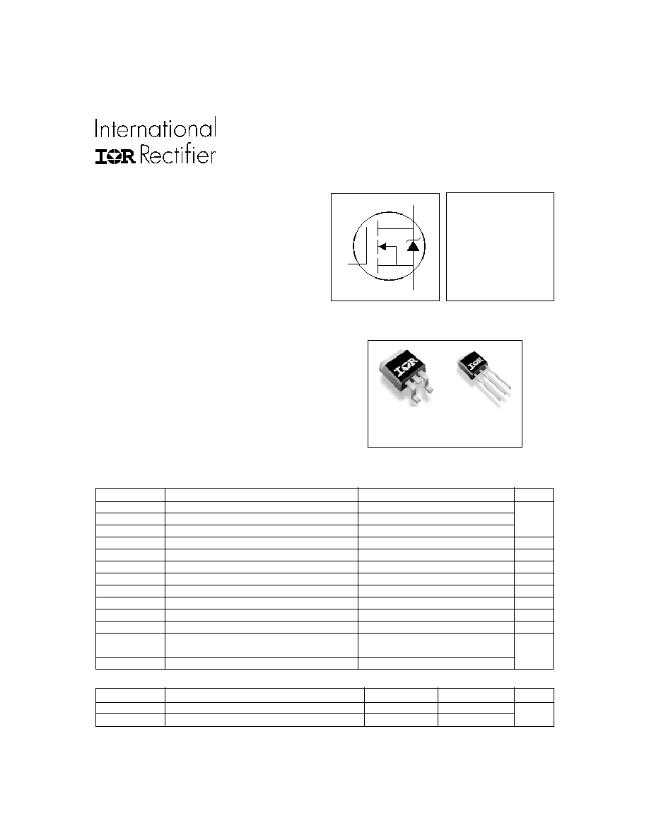
IRF840LCS
IRF840LCL
D
2
Pak
IRF840LCS
TO-262
IRF840LCL
IRF840LCS/LCL
2
www.irf.com
Parameter
Min. Typ. Max. Units
Conditions
I
S
Continuous Source Current
MOSFET symbol
(Body Diode)
showing the
I
SM
Pulsed Source Current
integral reverse
(Body Diode)
p-n junction diode.
V
SD
Diode Forward Voltage
2.0
V
T
J
= 25°C, I
S
= 8.0A, V
GS
= 0V
t
rr
Reverse Recovery Time
490
740
ns
T
J
= 25°C, I
F
= 8.0A
Q
r r
Reverse Recovery Charge
3.0
4.5
µC
di/dt = 100A/µs
t
on
Forward Turn-On Time
Intrinsic turn-on time is negligible (turn-on is dominated by L
S
+L
D
)
Starting T
J
= 25°C, L = 14mH
R
G
= 25
, I
AS
= 8.0A. (See Figure 12)
Repetitive rating; pulse width limited by
max. junction temperature. (See fig. 11)
Notes:
I
SD
8.0A, di/dt
100A/µs, V
DD
V
(BR)DSS
,
T
J
150°C
Pulse width
300µs; duty cycle
2%.
Uses IRF840LC data and test conditions
** When mounted on 1" square PCB (FR-4 or G-10 Material).
For recommended soldering techniques refer to application note #AN-994.
S
D
G
Source-Drain Ratings and Characteristics
8.0
28
A
Parameter
Min. Typ. Max. Units
Conditions
V
(BR)DSS
Drain-to-Source Breakdown Voltage
500
V
V
GS
= 0V, I
D
= 250µA
V
(BR)DSS
/
T
J
Breakdown Voltage Temp. Coefficient
0.63
V/°C
Reference to 25°C, I
D
= 1mA
R
DS(on)
Static Drain-to-Source On-Resistance
0.85
V
GS
= 10V, I
D
= 4.8A
V
GS(th)
Gate Threshold Voltage
2.0
4.0
V
V
DS
= V
GS
, I
D
= 250µA
g
fs
Forward Transconductance
4.0
S
V
DS
= 50V, I
D
= 4.8A
25
µA
V
DS
= 500V, V
GS
= 0V
250
V
DS
= 400V, V
GS
= 0V, T
J
= 125°C
Gate-to-Source Forward Leakage
100
V
GS
= 20V
Gate-to-Source Reverse Leakage
-100
nA
V
GS
= -20V
Q
g
Total Gate Charge
39
I
D
= 8.0A
Q
gs
Gate-to-Source Charge
10
nC
V
DS
= 400V
Q
gd
Gate-to-Drain ("Miller") Charge
19
V
GS
= 10V, See Fig. 6 and 13
t
d(on)
Turn-On Delay Time
12
V
DD
= 250V
t
r
Rise Time
25
I
D
= 8.0A
t
d(off)
Turn-Off Delay Time
27
R
G
= 9.1
t
f
Fall Time
19
R
D
= 30
, See Fig. 10
Between lead,
and center of die contact
C
iss
Input Capacitance
1100
V
GS
= 0V
C
oss
Output Capacitance
170
pF
V
DS
= 25V
C
rss
Reverse Transfer Capacitance
18
= 1.0MHz, See Fig. 5
Electrical Characteristics @ T
J
= 25°C (unless otherwise specified)
I
GSS
ns
I
DSS
Drain-to-Source Leakage Current
nH
7.5
L
S
Internal Source Inductance
IRF840LCS/LCL
www.irf.com
3
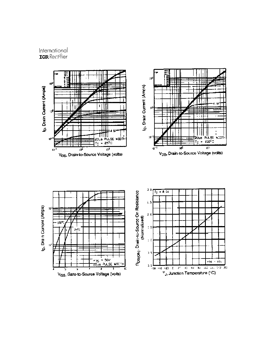
Fig 4. Normalized On-Resistance
Vs. Temperature
Fig 2. Typical Output Characteristics
Fig 1. Typical Output Characteristics
Fig 3. Typical Transfer Characteristics
IRF840LCS/LCL
4
www.irf.com
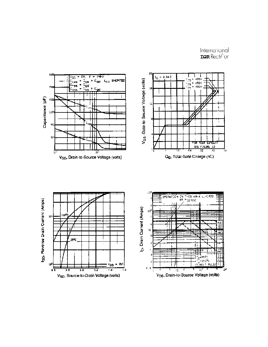
Fig 8. Maximum Safe Operating Area
Fig 6. Typical Gate Charge Vs.
Gate-to-Source Voltage
Fig 5. Typical Capacitance Vs.
Drain-to-Source Voltage
Fig 7. Typical Source-Drain Diode
Forward Voltage
IRF840LCS/LCL
www.irf.com
5
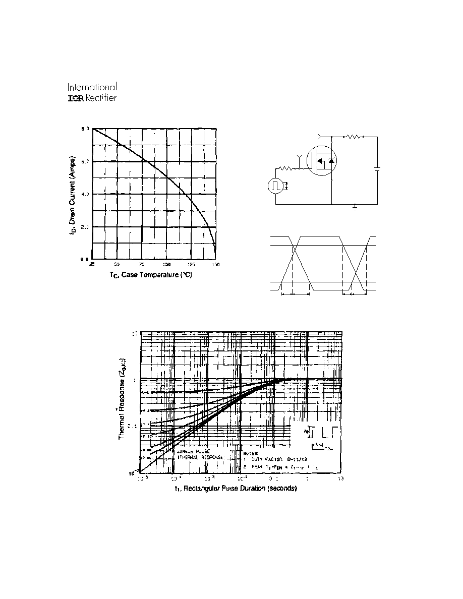
Fig 10a. Switching Time Test Circuit
V
DS
90%
10%
V
GS
t
d(on)
t
r
t
d(off)
t
f
Fig 10b. Switching Time Waveforms
V
DS
Pulse Width
1
µs
Duty Factor
0.1 %
R
D
V
GS
R
G
D.U.T.
10V
+
-
V
DD
Fig 11. Maximum Effective Transient Thermal Impedance, Junction-to-Case
Fig 9. Maximum Drain Current Vs.
Case Temperature