Äîêóìåíòàöèÿ è îïèñàíèÿ www.docs.chipfind.ru
IRFB16N60L
SMPS MOSFET
HEXFET
®
Power MOSFET
Features and Benefits
· SuperFast body diode eliminates the need for external
diodes in ZVS applications.
· Lower Gate charge results in simpler drive requirements.
· Enhanced dv/dt capabilities offer improved ruggedness.
· Higher Gate voltage threshold offers improved noise immunity
.
TO-220AB
10/19/04
www.irf.com
1
S
D
G
Applications
· Zero Voltage Switching SMPS
· Telecom and Server Power Supplies
· Uninterruptible Power Supplies
· Motor Control applications
V
DSS
R
DS(on)
typ.
Trr
typ.
I
D
600V
385m
130ns
16A
Absolute Maximum Ratings
Parameter
Max.
Units
I
D
@ T
C
= 25°C Continuous Drain Current, V
GS
@ 10V
16
I
D
@ T
C
= 100°C Continuous Drain Current, V
GS
@ 10V
10
A
I
DM
Pulsed Drain Current
c
60
P
D
@T
C
= 25°C Power Dissipation
310
W
Linear Derating Factor
2.5
W/°C
V
GS
Gate-to-Source Voltage
±30
V
dv/dt
Peak Diode Recovery dv/dt
e
11
V/ns
T
J
Operating Junction and
-55 to + 150
T
STG
Storage Temperature Range
°C
Soldering Temperature, for 10 seconds
300 (1.6mm from case )
Mounting torque, 6-32 or M3 screw
1.1(10)
N·m (lbf·in)
Diode Characteristics
Symbol
Parameter
Min. Typ. Max. Units
Conditions
I
S
Continuous Source Current
16
MOSFET symbol
(Body Diode)
A
showing the
I
SM
Pulsed Source Current
60
integral reverse
(Body Diode)
Ã
c
p-n junction diode.
V
SD
Diode Forward Voltage
1.5
V
T
J
= 25°C, I
S
= 16A, V
GS
= 0V
f
t
rr
Reverse Recovery Time
130
200
ns T
J
= 25°C, I
F
= 16A
240
360
T
J
= 125°C, di/dt = 100A/µs
f
Q
rr
Reverse Recovery Charge
450
670
nC T
J
= 25°C, I
S
= 16A, V
GS
= 0V
f
1080 1620
T
J
= 125°C, di/dt = 100A/µs
f
I
RRM
Reverse Recovery Current
5.8
8.7
A
T
J
= 25°C
t
on
Forward Turn-On Time
Intrinsic turn-on time is negligible (turn-on is dominated by LS+LD)
PD - 94631A
IRFB16N60L
2
www.irf.com
Notes:
Repetitive rating; pulse width limited by
max. junction temperature. (See Fig. 12)
Starting T
J
= 25°C, L = 2.5mH, R
G
= 25
,
I
AS
= 16A.(See Figure 14a)
I
SD
16A, di/dt
650A/µs, V
DD
V
(BR)DSS
,
T
J
150°C.
Pulse width
300µs; duty cycle
2%.
C
oss
eff. is a fixed capacitance that gives the same charging time
as C
oss
while V
DS
is rising from 0 to 80% V
DSS
.
C
oss
eff.(ER) is a fixed capacitance that stores the same energy
as C
oss
while V
DS
is rising from 0 to 80% V
DSS
.
R
is measured at T
J
approximately 90°C
Static @ T
J
= 25°C (unless otherwise specified)
Symbol
Parameter
Min. Typ. Max. Units
V
(BR)DSS
Drain-to-Source Breakdown Voltage
600
V
V
(BR)DSS
/
T
J
Breakdown Voltage Temp. Coefficient
0.39
V/°C
R
DS(on)
Static Drain-to-Source On-Resistance
385
460
m
V
GS(th)
Gate Threshold Voltage
3.0
5.0
V
I
DSS
Drain-to-Source Leakage Current
50
µA
2.0
mA
I
GSS
Gate-to-Source Forward Leakage
100
nA
Gate-to-Source Reverse Leakage
-100
R
G
Internal Gate Resistance
0.79
Dynamic @ T
J
= 25°C (unless otherwise specified)
Symbol
Parameter
Min. Typ. Max. Units
gfs
Forward Transconductance
8.3
S
Q
g
Total Gate Charge
100
Q
gs
Gate-to-Source Charge
30
nC
Q
gd
Gate-to-Drain ("Miller") Charge
46
t
d(on)
Turn-On Delay Time
20
t
r
Rise Time
44
ns
t
d(off)
Turn-Off Delay Time
28
t
f
Fall Time
5.5
C
iss
Input Capacitance
2720
C
oss
Output Capacitance
260
C
rss
Reverse Transfer Capacitance
20
pF
C
oss
eff.
Effective Output Capacitance
120
C
oss
eff. (ER)
Effective Output Capacitance
100
(Energy Related)
Avalanche Characteristics
Symbol
Parameter
Typ.
Units
E
AS
Single Pulse Avalanche Energy.
d
mJ
I
AR
Avalanche Current
Ã
A
E
AR
Repetitive Avalanche Energy
mJ
Thermal Resistance
Symbol
Parameter
Typ.
Units
R
JC
Junction-to-Case
h
°C/W
R
JA
Junction-to-Ambient
h
62
Max.
0.4
V
DS
= 25V
= 1.0MHz, See Fig. 5
16
31
Max.
310
V
GS
= 0V,V
DS
= 0V to 480V
g
I
D
= 16A
R
G
= 1.8
V
GS
= 10V, See Fig. 11a & 11b
f
V
GS
= 0V
I
D
= 16A
V
DS
= 480V
V
GS
= 10V, See Fig. 7 & 15
f
V
DD
= 300V
V
GS
= 30V
f = 1MHz, open drain
Conditions
V
DS
= 50V, I
D
= 9.0A
V
GS
= -30V
V
DS
= V
GS
, I
D
= 250µA
V
DS
= 600V, V
GS
= 0V
V
DS
= 480V, V
GS
= 0V, T
J
= 125°C
Conditions
V
GS
= 0V, I
D
= 250µA
Reference to 25°C, I
D
= 1mA
V
GS
= 10V, I
D
= 9.0A
f
IRFB16N60L
www.irf.com
3
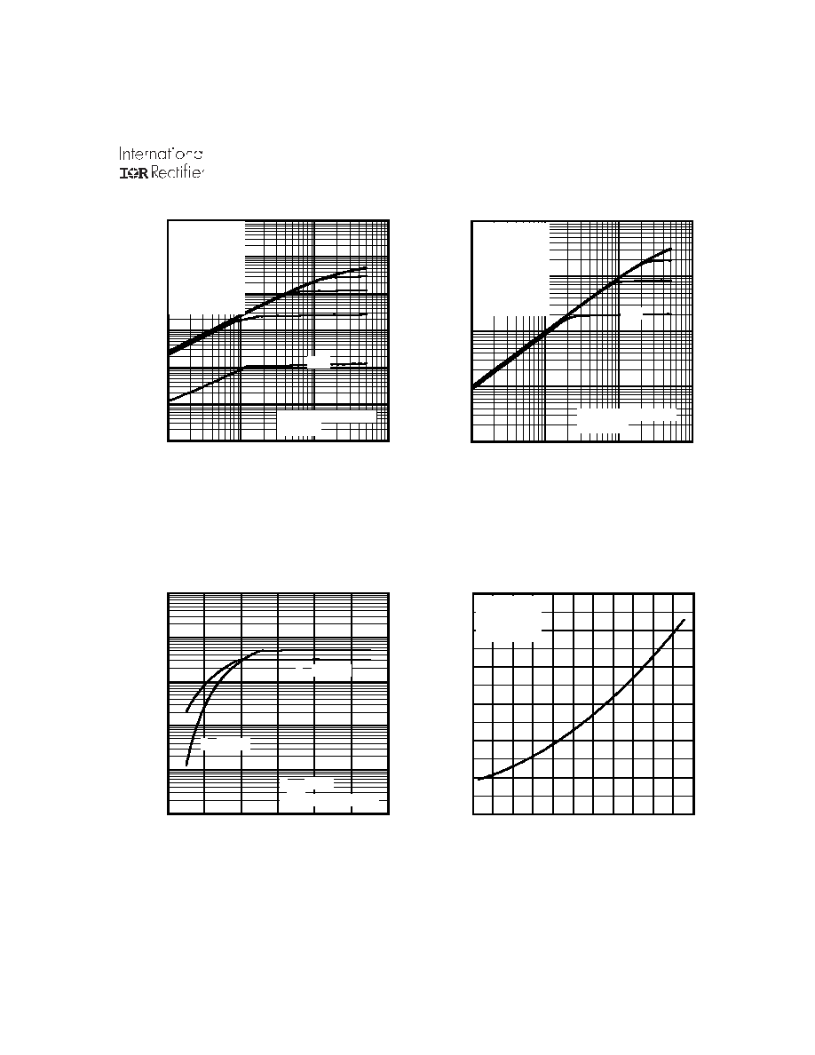
Fig 4. Normalized On-Resistance
vs. Temperature
Fig 2. Typical Output Characteristics
Fig 1. Typical Output Characteristics
Fig 3. Typical Transfer Characteristics
0.1
1
10
100
VDS, Drain-to-Source Voltage (V)
0.01
0.1
1
10
100
I D
,
D
r
a
i
n
-
t
o
-
S
o
u
r
c
e
C
u
r
r
e
n
t
(
A
)
5.0V
20µs PULSE WIDTH
Tj = 150°C
VGS
TOP
15V
12V
10V
9.0V
8.0V
7.0V
6.0V
BOTTOM
5.0V
0.1
1
10
100
VDS, Drain-to-Source Voltage (V)
0.001
0.01
0.1
1
10
100
1000
I D
,
D
r
a
i
n
-
t
o
-
S
o
u
r
c
e
C
u
r
r
e
n
t
(
A
)
5.0V
20µs PULSE WIDTH
Tj = 25°C
VGS
TOP
15V
12V
10V
9.0V
8.0V
7.0V
6.0V
BOTTOM
5.0V
4
6
8
10
12
14
16
VGS, Gate-to-Source Voltage (V)
0.01
0.1
1
10
100
1000
I D
,
D
r
a
i
n
-
t
o
-
S
o
u
r
c
e
C
u
r
r
e
n
t
(
)
TJ = 25°C
TJ = 150°C
VDS = 50V
20µs PULSE WIDTH
-60 -40 -20
0
20
40
60
80 100 120 140 160
TJ , Junction Temperature (°C)
0.0
0.5
1.0
1.5
2.0
2.5
3.0
R
D
S
(
o
n
)
,
D
r
a
i
n
-
t
o
-
S
o
u
r
c
e
O
n
R
e
s
i
s
t
a
n
c
e
(
N
o
r
m
a
l
i
z
e
d
)
ID = 15A
VGS = 10V
IRFB16N60L
4
www.irf.com
Fig 5. Typical Capacitance vs.
Drain-to-Source Voltage
Fig 8. Typical Source-Drain Diode
Forward Voltage
Fig 7. Typical Gate Charge vs.
Gate-to-Source Voltage
Fig 6. Typ. Output Capacitance
Stored Energy vs. V
DS
1
10
100
1000
VDS, Drain-to-Source Voltage (V)
1
10
100
1000
10000
100000
C
,
C
a
p
a
c
i
t
a
n
c
e
(
p
F
)
VGS = 0V, f = 1 MHZ
Ciss = Cgs + Cgd, Cds SHORTED
Crss = Cgd
Coss = Cds + Cgd
Coss
Crss
Ciss
0
100
200
300
400
500
600
700
VDS, Drain-to-Source Voltage (V)
0
5
10
15
20
25
E
n
e
r
g
y
(
µ
J
)
0
10
20
30
40
50
60
70
QG Total Gate Charge (nC)
0.0
2.0
4.0
6.0
8.0
10.0
12.0
V
G
S
,
G
a
t
e
-
t
o
-
S
o
u
r
c
e
V
o
l
t
a
g
e
(
V
)
VDS= 480V
VDS= 300V
VDS= 120V
ID= 15A
0.2
0.4
0.6
0.8
1.0
1.2
1.4
1.6
VSD, Source-to-Drain Voltage (V)
0.10
1.00
10.00
100.00
I S
D
,
R
e
v
e
r
s
e
D
r
a
i
n
C
u
r
r
e
n
t
(
A
)
TJ = 25°C
TJ = 150°C
VGS = 0V
IRFB16N60L
www.irf.com
5
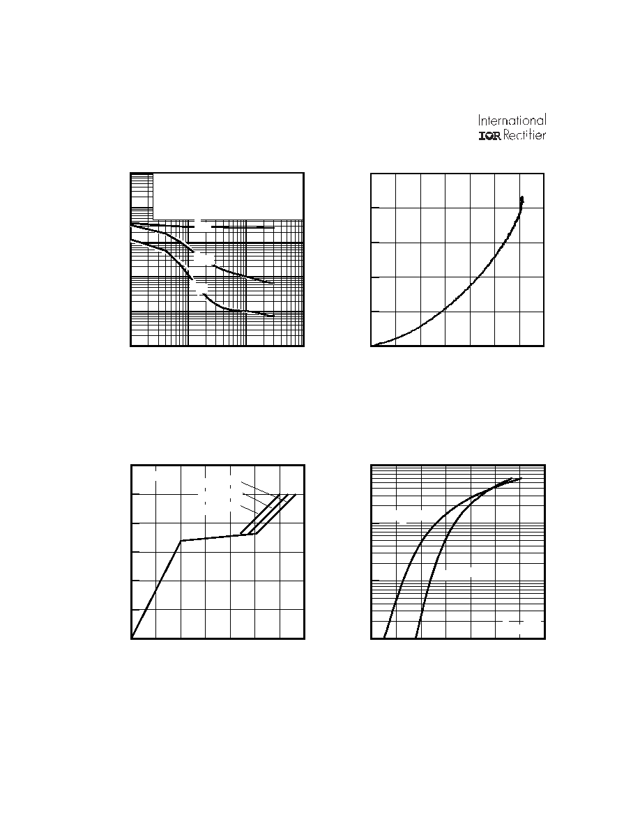
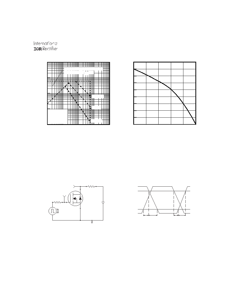
Fig 9. Maximum Safe Operating Area
Fig 10. Maximum Drain Current vs.
Case Temperature
V
DS
Pulse Width 1 µs
Duty Factor 0.1 %
R
D
V
GS
R
G
D.U.T.
10V
V
DD
Fig 11a. Switching Time Test Circuit
+
-
V
DS
90%
10%
V
GS
t
d(on)
t
r
t
d(off)
t
f
Fig 11b. Switching Time Waveforms
1
10
100
1000
10000
VDS, Drain-to-Source Voltage (V)
0.1
1
10
100
1000
I D
,
D
r
a
i
n
-
t
o
-
S
o
u
r
c
e
C
u
r
r
e
n
t
(
A
)
1msec
10msec
OPERATION IN THIS AREA
LIMITED BY R DS(on)
100µsec
Tc = 25°C
Tj = 150°C
Single Pulse
25
50
75
100
125
150
TC , Case Temperature (°C)
0
2
4
6
8
10
12
14
16
18
I D
,
D
r
a
i
n
C
u
r
r
e
n
t
(
A
)