IRFBC20S/L
PRELIMINARY
HEXFET
Æ
Power MOSFET
PD - 9.1014
Parameter
Typ.
Max.
Units
R
JC
Junction-to-Case
≠≠≠
2.5
R
JA
Junction-to-Ambient ( PCB Mounted,steady-state)**
≠≠≠
40
Thermal Resistance
∞C/W
Parameter
Max.
Units
I
D
@ T
C
= 25∞C
Continuous Drain Current, V
GS
@ 10V
2.2
I
D
@ T
C
= 100∞C
Continuous Drain Current, V
GS
@ 10V
1.4
A
I
DM
Pulsed Drain Current
8.0
P
D
@T
A
= 25∞C
Power Dissipation
3.1
W
P
D
@T
C
= 25∞C
Power Dissipation
50
W
Linear Derating Factor
0.40
W/∞C
V
GS
Gate-to-Source Voltage
± 20
V
E
AS
Single Pulse Avalanche Energy
84
mJ
I
AR
Avalanche Current
2.2
A
E
AR
Repetitive Avalanche Energy
5.0
mJ
dv/dt
Peak Diode Recovery dv/dt
3.0
V/ns
T
J
Operating Junction and
-55 to + 150
T
STG
Storage Temperature Range
Soldering Temperature, for 10 seconds
300 (1.6mm from case )
∞C
Absolute Maximum Ratings
V
DSS
= 600V
R
DS(on)
= 4.4
I
D
= 2.2A
2
D P a k
T O - 2 6 2
S
D
G
7/22/97
l
Surface Mount (IRFBC20S)
l
Low-profile through-hole (IRFBC20L)
l
Available in Tape & Reel (IRFBC20S)
l
Dynamic dv/dt Rating
l
150∞C Operating Temperature
l
Fast Switching
l
Fully Avalanche Rated
Third generation HEXFETs from international Rectifier provide the designer with the
best combination of fast switching, ruggedized device design, low on-resistance and
cost-effectiveness.
The D
2
Pak is a surface mount power package capable of the accommodatingdie sizes
up to HEX-4. It provides the highest power capability and the lowest possible on-
resistance in any existing surface mount package. The D
2
Pak is suitable for high
current applications because of its low internal connection resistance and can
dissipate up to 2.0W in a typical surface mount application. The through-hole version
(IRFBC20L) is available for low-profile applications.
Description

IRFBC20S/L
V
DD
=50V, starting T
J
= 25∞C, L =31mH
R
G
= 25
, I
AS
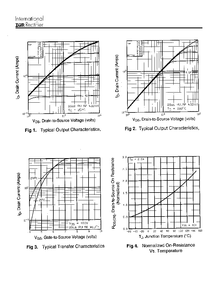
= 2.2A. (See Figure 12)
Repetitive rating; pulse width limited by
max. junction temperature. ( See fig. 11 )
Notes:
** When mounted on 1" square PCB (FR-4 or G-10 Material ).
For recommended footprint and soldering techniques refer to application note #AN-994.
I
SD
2.2A, di/dt
40A/µs, V
DD
V
(BR)DSS
,
T
J
150∞C
Pulse width
300µs; duty cycle
2%.
Uses IRFBC20 data and test conditions
Parameter
Min. Typ. Max. Units
Conditions
I
S
Continuous Source Current
MOSFET symbol
(Body Diode)
≠≠≠
≠≠≠
showing the
I
SM
Pulsed Source Current
integral reverse
(Body Diode)
≠≠≠
≠≠≠
p-n junction diode.
V
SD
Diode Forward Voltage
≠≠≠
≠≠≠
1.6
V
T
J
= 25∞C, I
S
= 2.2A, V
GS
= 0V
t
rr
Reverse Recovery Time
≠≠≠
290
580
ns
T
J
= 25∞C, I
F
= 2.0A
Q
rr
Reverse Recovery Charge
≠≠≠
0.67
1.3
µC
di/dt = 100A/µs
t
on
Forward Turn-On Time
Intrinsic turn-on time is negligible (turn-on is dominated by L
S
+L
D
)
Source-Drain Ratings and Characteristics
A
Parameter
Min. Typ. Max. Units
Conditions
V
(BR)DSS
Drain-to-Source Breakdown Voltage
600
≠≠≠
≠≠≠
V
V
GS
= 0V, I
D
= 250µA
V
(BR)DSS
/
T
J
Breakdown Voltage Temp. Coefficient
≠≠≠
0.88
≠≠≠
V/∞C
Reference to 25∞C, I
D
=1mA
R
DS(on)
Static Drain-to-Source On-Resistance
≠≠≠
≠≠≠
4.4
V
GS
=10V, I
D
= 1.3A
V
GS(th)
Gate Threshold Voltage
2.0
≠≠≠
4.0
V
V
DS
= V
GS
, I
D
= 250µA
g
fs
Forward Transconductance
1.4
≠≠≠
≠≠≠
S
V
DS
= 50V, I
D
= 1.3A
≠≠≠
≠≠≠
100
µA
V
DS
= 600V, V
GS
= 0V
≠≠≠
≠≠≠
500
V
DS
= 480V, V
GS
= 0V, T
J
= 125∞C
Gate-to-Source Forward Leakage
≠≠≠
≠≠≠
100
V
GS
= 20V
Gate-to-Source Reverse Leakage
≠≠≠
≠≠≠
-100
nA
V
GS
= -20V
Q
g
Total Gate Charge
≠≠≠
≠≠≠
18
I
D
= 2.0A
Q
gs
Gate-to-Source Charge
≠≠≠
≠≠≠
3.0
nC
V
DS
= 360V
Q
gd
Gate-to-Drain ("Miller") Charge
≠≠≠
≠≠≠
8.9
V
GS
= 10V, See Fig. 6 and 13
t
d(on)
Turn-On Delay Time
≠≠≠
10
≠≠≠
V
DD
= 300V
t
r
Rise Time
≠≠≠
23
≠≠≠
I
D
= 2.0A
t
d(off)
Turn-Off Delay Time
≠≠≠
30
≠≠≠
R
G
= 18
t
f
Fall Time
≠≠≠
25
≠≠≠
R
D
= 150
,
See Fig. 10
Between lead,
≠≠≠
≠≠≠
and center of die contact
C
iss
Input Capacitance
≠≠≠
350
≠≠≠
V
GS
= 0V
C
oss
Output Capacitance
≠≠≠
48
≠≠≠
pF
V
DS
= 25V
C
rss
Reverse Transfer Capacitance
≠≠≠
8.6
≠≠≠
= 1.0MHz, See Fig. 5
Electrical Characteristics @ T
J
= 25∞C (unless otherwise specified)
I
GSS
ns
I
DSS
Drain-to-Source Leakage Current
nH
7.5
L
S
Internal Source Inductance
2.2
8.0
S
D
G