 | ÐлекÑÑоннÑй компоненÑ: IRFDC20 | СкаÑаÑÑ:  PDF PDF  ZIP ZIP |
Äîêóìåíòàöèÿ è îïèñàíèÿ www.docs.chipfind.ru
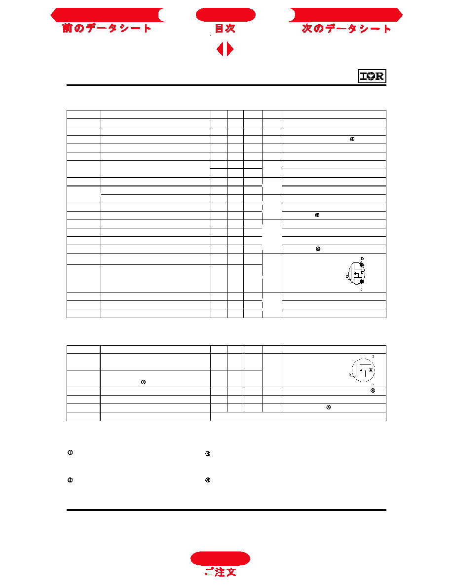
Parameter
Max.
Units
I
D
@ T
C
= 25°C
Continuous Drain Current, V
GS
@ 10 V
0.32
I
D
@ T
C
= 100°C
Continuous Drain Current, V
GS
@ 10 V
0.20
A
I
DM
Pulsed Drain Current
2.6
P
D
@T
C
= 25°C
Power Dissipation
1.0
W
Linear Derating Factor
0.0083
W/°C
V
GS
Gate-to-Source Voltage
±20
V
E
AS
Single Pulse Avalanche Energy
50
mJ
I
AR
Avalanche Current
0.32
A
E
AR
Repetitive Avalanche Energy
0.10
mJ
dv/dt
Peak Diode Recovery dv/dt
3.0
V/ns
T
J
Operating Junction and
-55 to + 150
T
STG
Storage Temperature Range
°C
Soldering Temperature, for 10 seconds
300 (1.6mm from case)
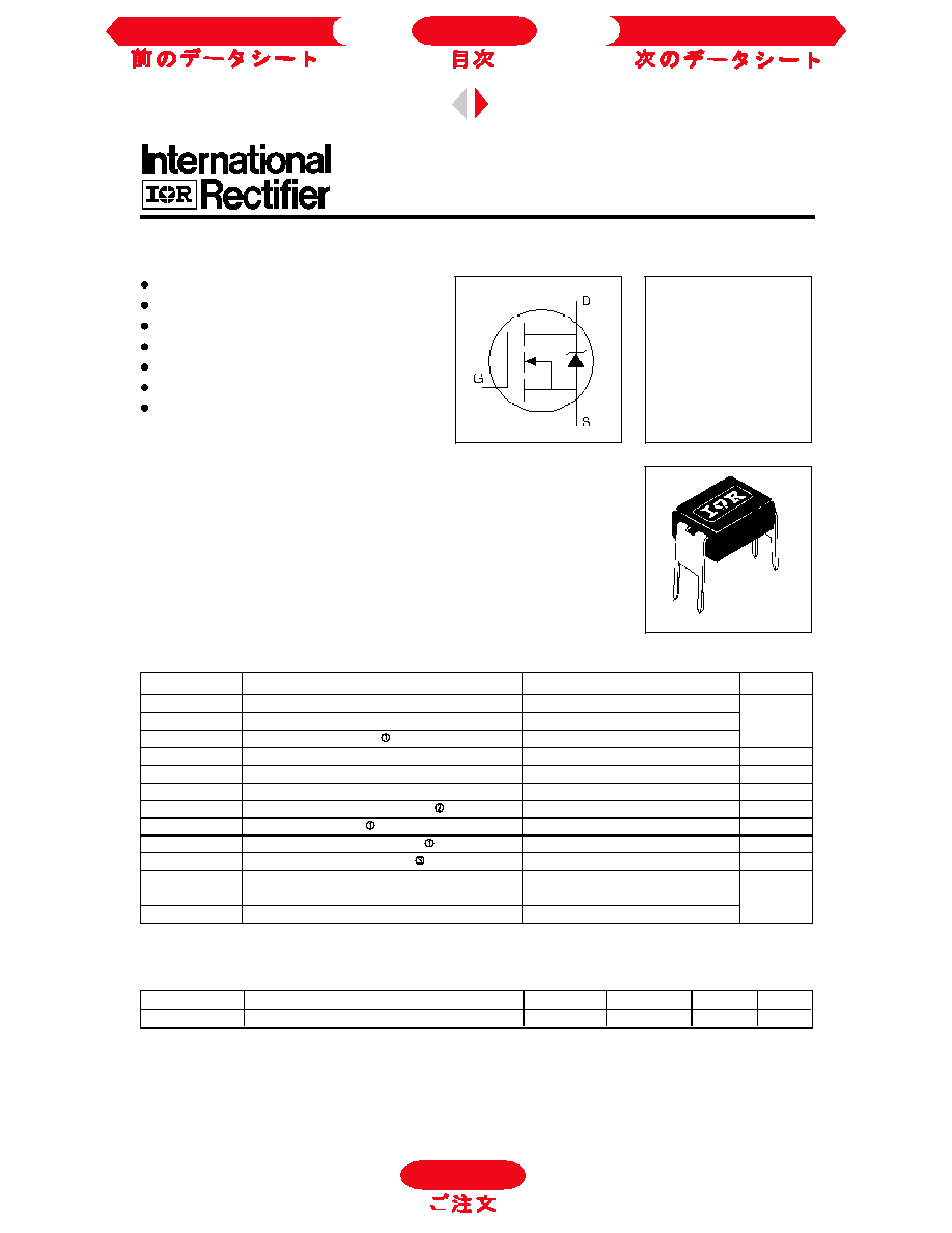
IRFDC20
HEXFET
®
Power MOSFET
PD -9.1228
Revision 0
V
DSS
= 600V
R
DS(on)
= 4.4
I
D
= 0.32A
Absolute Maximum Ratings
Thermal Resistance
Parameter
Min.
Typ.
Max.
Units
R
JA
Junction-to-Ambient
--
--
120
°C/W
Dynamic dv/dt Rating
Repetitive Avalanche Rated
For Automatic Insertion
End Stackable
Fast Switching
Ease of paralleling
Simple Drive Requirements
Third Generation HEXFETs from International Rectifier provide the designer
with the best combination of fast switching, ruggedized device design, low on-
resistance and cost-effectiveness.
The 4-pin DIP package is a low-cost machine-insertable case style which can be
stacked in multiple combinations on standard 0.1 inch pin centers. The dual drain
serves as a thermal link to the mounting surface for power dissipation levels up to
1 watt.
Description
A
HD-1
Next Data Sheet
Index
Previous Datasheet
To Order
Parameter
Min. Typ. Max. Units Conditions
V
(BR)DSS
Drain-to-Source Breakdown Voltage
600
--
--
V
V
GS
= 0V, ID = 250µA
V
(BR)DSS
/
T
J
Breakdown Voltage Temp. Coefficient
--
0.88
--
V/°C Reference to 25°C, I
D
= 1mA
R
DS(on)
Static Drain-to-Source On-Resistance
--
--
4.4
V
GS
= 10.0V, I
D
= 0.19A
V
GS(th)
Gate Threshold Voltage
2.0
--
4.0
V
V
DS
= V
GS
, I
D
= 250µA
g
fs
Forward Transconductance
1.4
--
--
S
V
DS
= 50V, I
D
= 1.3A
I
DSS
Drain-to-Source Leakage Current
--
--
25
V
DS
= 600V, V
GS
= 0V
--
--
250
V
DS
= 480V, V
GS
= 0V, T
J
= 125°C
I
GSS
Gate-to-Source Forward Leakage
--
--
100
V
GS
= 20V
Gate-to-Source Reverse Leakage
--
--
-100
V
GS
= -20V
Q
g
Total Gate Charge
--
--
18
I
D
= 2.0A
Q
gs
Gate-to-Source Charge
--
--
3.0
nC
V
DS
= 360V
Q
gd
Gate-to-Drain ("Miller") Charge
--
--
8.9
V
GS
= 10V
t
d(on)
Turn-On Delay Time
--
10
--
V
DD
= 300V
t
r
Rise Time
--
23
--
I
D
= 2.0A
t
d(off)
Turn-Off Delay Time
--
30
--
R
G
= 18
t
f
Fall Time
--
25
--
R
D
= 150
L
D
Internal Drain Inductance
--
4.0
--
Between lead,
6mm (0.25in.)
L
S
Internal Source Inductance
--
6.0
--
from package
and center of
die contact
C
iss
Input Capacitance
--
350
--
V
GS
= 0V
C
oss
Output Capacitance
--
48
--
pF
V
DS
= 25V
C
rss
Reverse Transfer Capacitance
--
8.6
--
= 1.0MHz
IRFDC20
Notes:
Parameter
Min. Typ. Max. Units Conditions
I
S
Continuous Source Current
MOSFET symbol
(Body Diode)
showing the
I
SM
Pulsed Source Current
integral reverse
(Body Diode)
p-n junction diode.
V
SD
Diode Forward Voltage
--
--
1.6
V
T
J
= 25°C, I
S
= 0.32A, V
GS
= 0V
t
rr
Reverse Recovery Time
--
290
580
ns
T
J
= 25°C, I
F
= 2.0A
Q
rr
Reverse RecoveryCharge
--
0.67
1.3
µC
di/dt = 100A/µs
t
on
Forward Turn-On Time
Repetitive rating; pulse width limited by
max. junction temperature.
V
DD
= 50V, starting T
J
= 25°C, L = 54mH
R
G
= 25
, I
AS
= 1.3A.
I
SD
4.4A, di/dt
90A/µs, V
DD
V
(BR)DSS
,
T
J
150°C
Pulse width
300µs; duty cycle
2%.
Source-Drain Ratings and Characteristics
Electrical Characteristics @ T
J
= 25°C (unless otherwise specified)
Intrinsic turn-on time is negligible (turn-on is dominated by L
S
+L
D
)
--
--
2.6
--
--
0.32
A
µA
nA
ns
nH
Next Data Sheet
Index
Previous Datasheet
To Order
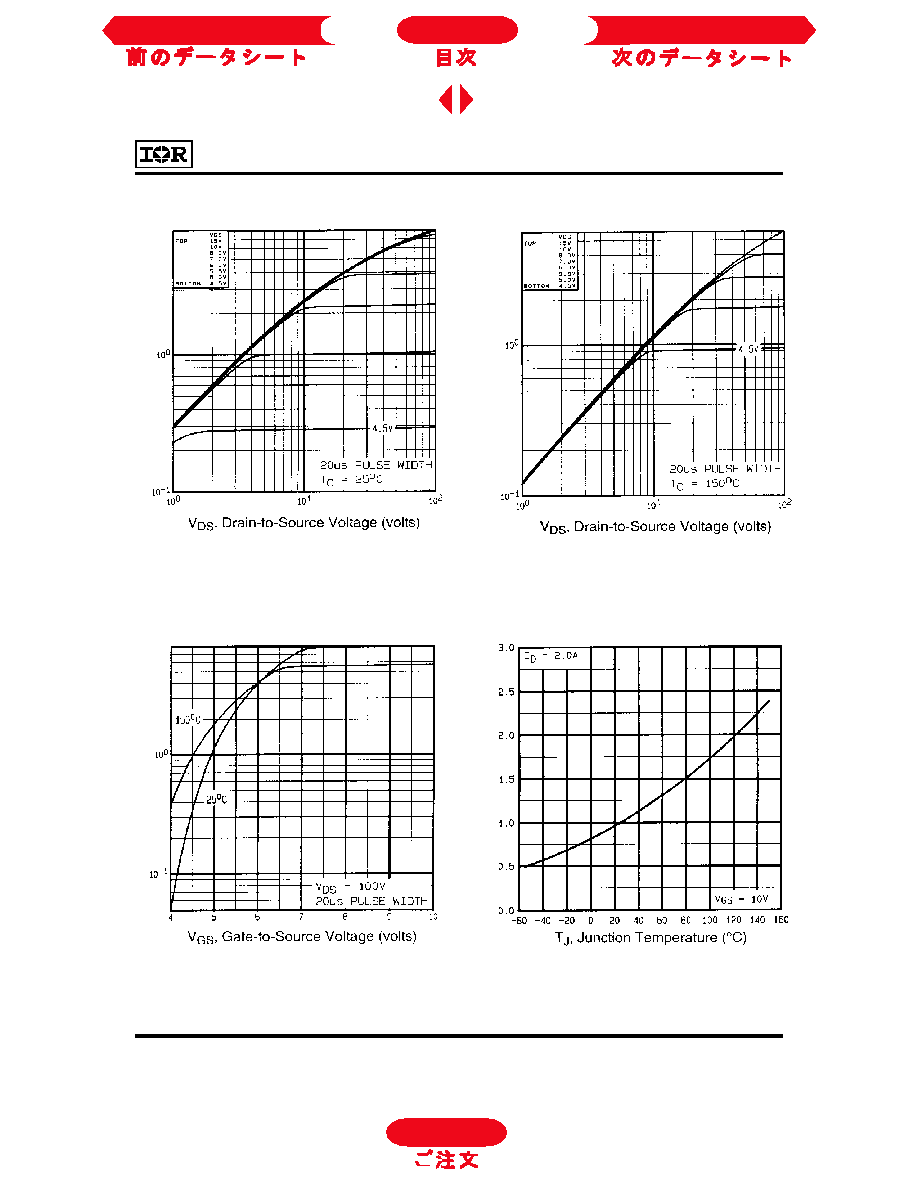
Fig 3. Typical Transfer Characteristics
Fig 4. Normalized On-Resistance
Vs. Temperature
IRFDC20
Fig 1. Typical Output Characteristics,
T
C
= 25
o
C
Fig 2. Typical Output Characteristics,
T
C
= 150
o
C
R
D
S
(
o
n
)
,
D
r
a
i
n
-
t
o
-
S
o
u
r
c
e
O
n
R
e
s
i
s
t
a
n
c
e
(
N
o
r
m
a
l
i
z
e
d
)
I
D
,
D
r
a
i
n
C
u
r
r
e
n
t
(
A
m
p
s
)
I
D
,
D
r
a
i
n
C
u
r
r
e
n
t
(
A
m
p
s
)
I
D
,
D
r
a
i
n
C
u
r
r
e
n
t
(
A
m
p
s
)
To Order
Next Data Sheet
Index
Previous Datasheet
IRFDC20
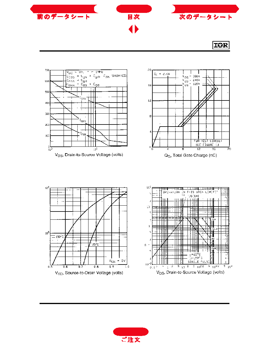
Fig 7. Typical Source-Drain Diode
Forward Voltage
Fig 8. Maximum Safe Operating Area
Fig 5. Typical Capacitance Vs.
Drain-to-Source Voltage
Fig 6. Typical Gate Charge Vs.
Gate-to-Source Voltage
C
a
p
a
c
i
t
a
n
c
e
(
p
F
)
V
G
S
,
G
a
t
e
-
t
o
-
S
o
u
r
c
e
V
o
l
t
a
g
e
(
v
o
l
t
s
)
I
S
D
,
R
e
v
e
r
s
e
D
r
a
i
n
C
u
r
r
e
n
t
(
A
m
p
s
)
I
D
,
D
r
a
i
n
C
u
r
r
e
n
t
(
A
m
p
s
)
To Order
Next Data Sheet
Index
Previous Datasheet
IRFDC20
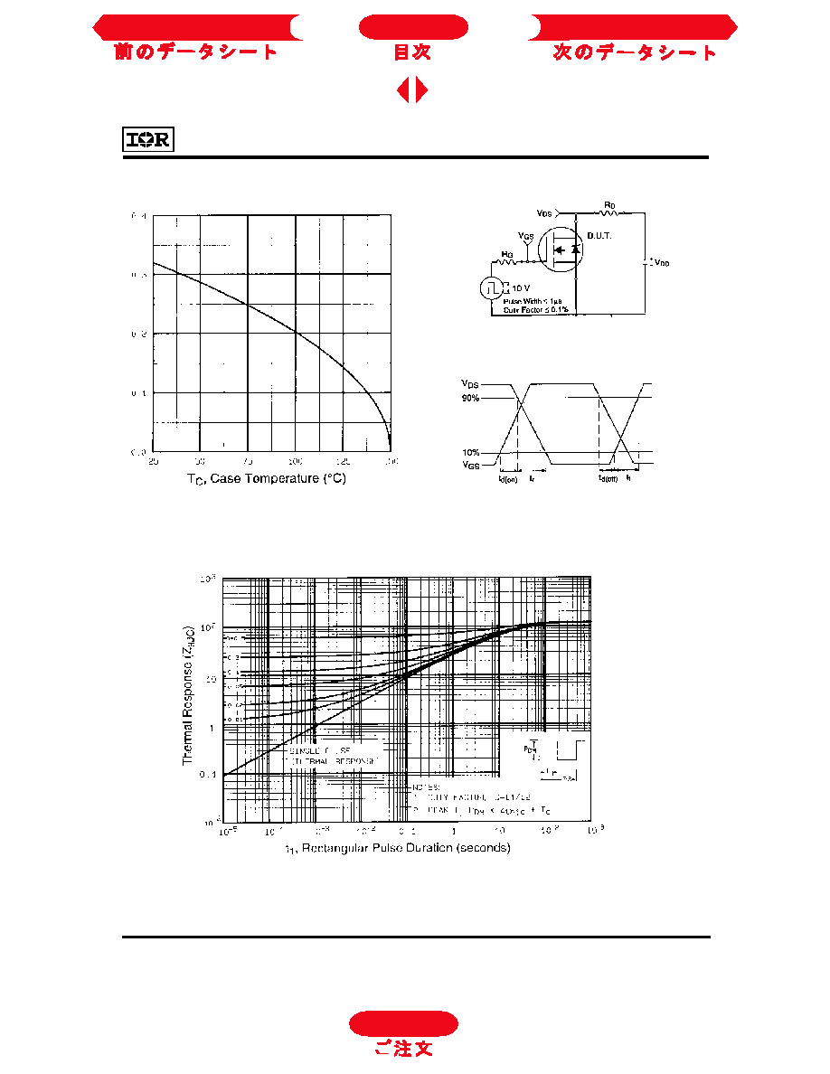
Fig 10a. Switching Time Test Circuit
Fig 9. Maximum Drain Current Vs.
Case Temperature
Fig 10b. Switching Time Waveforms
Fig 11. Maximum Effective Transient Thermal Impedance, Junction-to-Case
I
D
,
D
r
a
i
n
C
u
r
r
e
n
t
(
A
m
p
s
)
To Order
Next Data Sheet
Index
Previous Datasheet