 | ÐлекÑÑоннÑй компоненÑ: IRFI9610G | СкаÑаÑÑ:  PDF PDF  ZIP ZIP |
Äîêóìåíòàöèÿ è îïèñàíèÿ www.docs.chipfind.ru
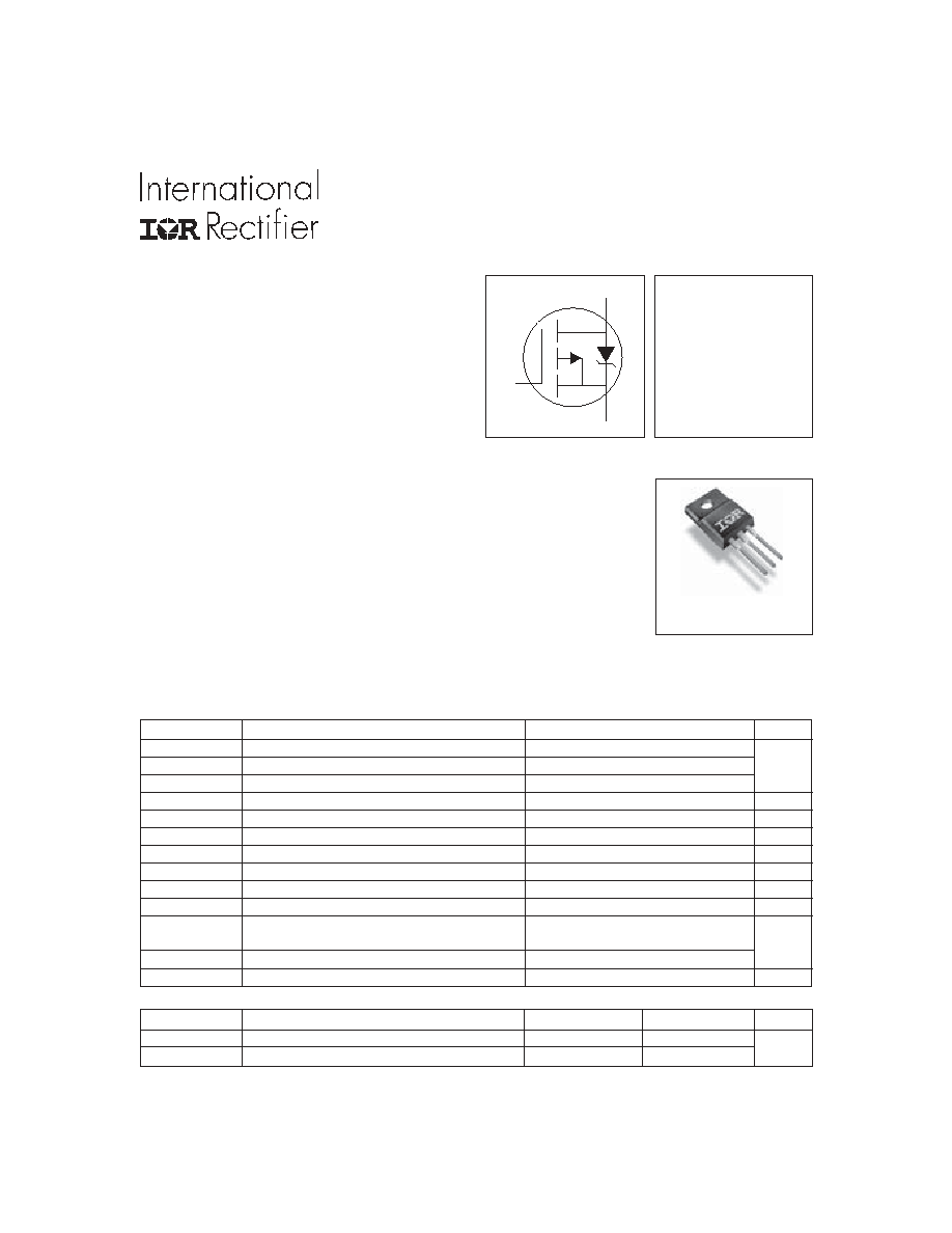
IRFI9610G
HEXFET
®
Power MOSFET
PD - 94577
Third Generation HEXFETs from International Rectifier provide the designer with the
best combination of fast switching, ruggedized device design, low on-resistance and
cost-effectiveness.Third Generation HEXFETs from International Rectifier provide the
designer with the best combination of fast switching, ruggedized device design, low
on-resistance and cost-effectiveness.
The TO-220 Fullpak eliminates the need for additional insulating hardware in commercial-
industrial applications. The moulding compound used provides a high isolation capability
and a low thermal resistance between the tab and external heatsink. This isolation is
equivalent to using a 100 micron mica barrier with standard TO-220 product. The Fullpak
is mounted to a heatsink using a single clip or by a single screw fixing.
Parameter
Max.
Units
I
D
@ T
C
= 25°C
Continuous Drain Current, V
GS
@ -10V
-2.0
I
D
@ T
C
= 100°C
Continuous Drain Current, V
GS
@ -10V
-1.3
A
I
DM
Pulsed Drain Current
-8.0
P
D
@T
C
= 25°C
Power Dissipation
27
W
Linear Derating Factor
0.22
W/°C
V
GS
Gate-to-Source Voltage
± 20
V
E
AS
Single Pulse Avalanche Energy
100
mJ
I
AR
Avalanche Current
-2.0
A
E
AR
Repetitive Avalanche Energy
2.7
mJ
dv/dt
Peak Diode Recovery dv/dt
-11
V/ns
T
J
Operating Junction and
-55 to + 150
T
STG
Storage Temperature Range
Soldering Temperature, for 10 seconds
300 (1.6mm from case )
°C
Mounting torque, 6-32 or M3 screw10 lbfin (1.1Nm)
Absolute Maximum Ratings
V
DSS
= -200V
R
DS(on)
= 3.0
I
D
= -2.0A
l
Isolated Package
l
High Voltage Isolation=2.5KVRMS
l
Sink to Lead Creepage Dist.=4.8mm
l
P-Channel
l
Dynamic dv/dt Rating
l
Low thermal Resistance
Description
10/28/02
S
D
G
Parameter
Typ.
Max.
Units
R
JC
Junction-to-Case
4.6
R
JA
Junction-to-Ambient
65
Thermal Resistance
°C/W
TO-220 Full-Pak
IRFI9610G
Parameter
Min. Typ. Max. Units
Conditions
I
S
Continuous Source Current
MOSFET symbol
(Body Diode)
showing the
I
SM
Pulsed Source Current
integral reverse
(Body Diode)
p-n junction diode.
V
SD
Diode Forward Voltage
-5.8
V
T
J
= 25°C, I
S
= -2.0A, V
GS
= 0V
t
rr
Reverse Recovery Time
130 200
ns
T
J
= 25°C, I
F
= -2.0A
Q
rr
Reverse Recovery Charge
700 1050
nC
di/dt = -100A/µs
t
on
Forward Turn-On Time
Intrinsic turn-on time is negligible (turn-on is dominated by L
S
+L
D
)
Parameter
Min. Typ. Max. Units
Conditions
V
(BR)DSS
Drain-to-Source Breakdown Voltage
-200
V
V
GS
= 0V, I
D
= -250µA
V
(BR)DSS
/
T
J
Breakdown Voltage Temp. Coefficient -0.22
V/°C Reference to 25°C, I
D
= -1mA
R
DS(on)
Static Drain-to-Source On-Resistance
3.0
V
GS
= -10V, I
D
= -1.2A
V
GS(th)
Gate Threshold Voltage
-2.0
-4.0
V
V
DS
= V
GS
, I
D
= -250µA
g
fs
Forward Transconductance
0.7
S
V
DS
= -50V, I
D
= -1.2A
-100
µA
V
DS
= -200V, V
GS
= 0V
-500
V
DS
= -160V, V
GS
= 0V, T
J
= 125°C
Gate-to-Source Forward Leakage
100
V
GS
= 20V
Gate-to-Source Reverse Leakage
-100
nA
V
GS
= -20V
Q
g
Total Gate Charge
13
I
D
= -2.0A
Q
gs
Gate-to-Source Charge
3.2
nC
V
DS
= -160V
Q
gd
Gate-to-Drain ("Miller") Charge
7.3
V
GS
= -10V, See Fig. 6 and 13
t
d(on)
Turn-On Delay Time
12
V
DD
= -100V
t
r
Rise Time
17
I
D
= -2.0A
t
d(off)
Turn-Off Delay Time
19
R
G
= 24
t
f
Fall Time
15
V
GS
= -10V
,
See Fig. 10
Between lead,
6mm (0.25in.)
from package
and center of die contact
C
iss
Input Capacitance
180
V
GS
= 0V
C
oss
Output Capacitance
66
pF
V
DS
= -25V
C
rss
Reverse Transfer Capacitance
12
= 1.0MHz, See Fig. 5
nH
Electrical Characteristics @ T
J
= 25°C (unless otherwise specified)
L
D
Internal Drain Inductance
L
S
Internal Source Inductance
I
GSS
ns
4.5
7.5
I
DSS
Drain-to-Source Leakage Current
Repetitive rating; pulse width limited by
max. junction temperature. ( See fig. 11 )
I
SD
-2.0A, di/dt
-250A/µs, V
DD
V
(BR)DSS
,
T
J
150°C
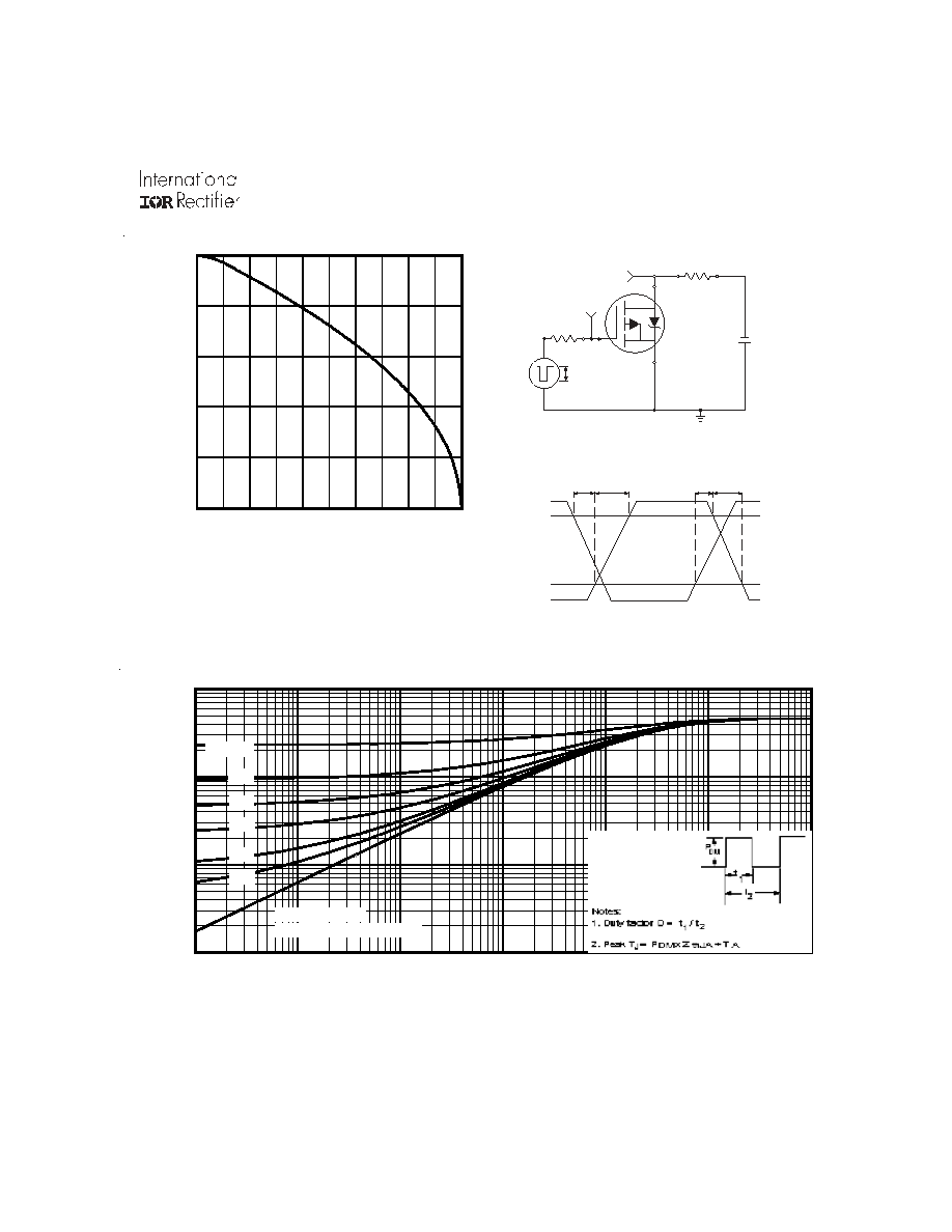
Notes:
Starting T
J
= 25°C, L = 51mH
R
G
= 25
, I
AS
= -2.0A. (See Figure 12)
Pulse width
300µs; duty cycle
2%.
t =60s, f=60Hz.
S
D
G
Source-Drain Ratings and Characteristics
A
S
D
G
-2.0
-8.0
IRFI9610G
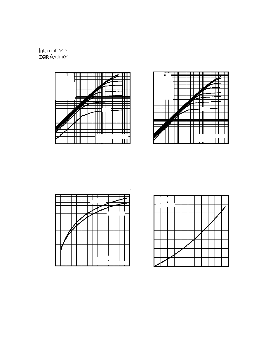
Fig 4. Normalized On-Resistance
Vs. Temperature
Fig 2. Typical Output Characteristics,
T
J
= 150
o
C
Fig 1. Typical Output Characteristics,
T
J
= 25
o
C
Fig 3. Typical Transfer Characteristics
0.1
1
10
100
-VDS, Drain-to-Source Voltage (V)
0.01
0.1
1
10
-
I D
,
D
r
a
i
n
-
t
o
-
S
o
u
r
c
e
C
u
r
r
e
n
t
(
A
)
-4.5V
20µs PULSE WIDTH
Tj = 25°C
VGS
TOP -15V
-10V
-8.0V
-7.0V
-6.0V
-5.5V
-5.0V
BOTTOM -4.5V
0.1
1
10
100
-VDS, Drain-to-Source Voltage (V)
0.01
0.1
1
10
-
I D
,
D
r
a
i
n
-
t
o
-
S
o
u
r
c
e
C
u
r
r
e
n
t
(
A
)
-4.5V
20µs PULSE WIDTH
Tj = 150°C
VGS
TOP -15V
-10V
-8.0V
-7.0V
-6.0V
-5.5V
-5.0V
BOTTOM -4.5V
4.0
5.0
6.0
7.0
8.0
9.0
10.0
11.0
-VGS, Gate-to-Source Voltage (V)
0
1
10
-
I D
,
D
r
a
i
n
-
t
o
-
S
o
u
r
c
e
C
u
r
r
e
n
t
(
)
TJ = 25°C
TJ = 150°C
VDS = -50V
20µs PULSE WIDTH
-60 -40 -20
0
20
40
60
80 100 120 140 160
TJ , Junction Temperature (°C)
0.5
1.0
1.5
2.0
2.5
R
D
S
(
o
n
)
,
D
r
a
i
n
-
t
o
-
S
o
u
r
c
e
O
n
R
e
s
i
s
t
a
n
c
e
(
N
o
r
m
a
l
i
z
e
d
)
ID = -2.0A
VGS = -10V
IRFI9610G
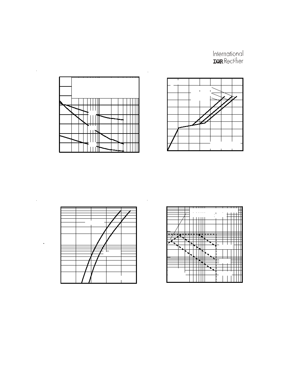
Fig 8. Maximum Safe Operating Area
Fig 6. Typical Gate Charge Vs.
Gate-to-Source Voltage
Fig 5. Typical Capacitance Vs.
Drain-to-Source Voltage
Fig 7. Typical Source-Drain Diode
Forward Voltage
0.0
1.0
2.0
3.0
4.0
5.0
-VSD, Source-toDrain Voltage (V)
0.1
1.0
10.0
-
I S
D
,
R
e
v
e
r
s
e
D
r
a
i
n
C
u
r
r
e
n
t
(
A
)
TJ = 25°C
TJ = 150°C
VGS = 0V
1
10
100
-VDS, Drain-to-Source Voltage (V)
0
50
100
150
200
250
300
350
400
C
,
C
a
p
a
c
i
t
a
n
c
e
(
p
F
)
Coss
Crss
Ciss
VGS = 0V, f = 1 MHZ
Ciss = Cgs + Cgd, Cds SHORTED
Crss = Cgd
Coss = Cds + Cgd
0
2
4
6
8
10
12
14
Q G Total Gate Charge (nC)
0
4
8
12
16
20
-
V
G
S
,
G
a
t
e
-
t
o
-
S
o
u
r
c
e
V
o
l
t
a
g
e
(
V
)
VDS= -160V
VDS= -100V
VDS= -40V
ID= -2.0A
FOR TEST CIRCUIT
SEE FIGURE 13
10
100
1000
-VDS , Drain-toSource Voltage (V)
0.1
1
10
100
-
I D
,
D
r
a
i
n
-
t
o
-
S
o
u
r
c
e
C
u
r
r
e
n
t
(
A
)
Tc = 25°C
Tj = 150°C
Single Pulse
1msec
10msec
OPERATION IN THIS AREA
LIMITED BY R DS(on)
100µsec
IRFI9610G
Fig 10a. Switching Time Test Circuit
Fig 10b. Switching Time Waveforms
Fig 11. Maximum Effective Transient Thermal Impedance, Junction-to-Case
Fig 9. Maximum Drain Current Vs.
Case Temperature
V
DS
-10V
Pulse Width
1
µs
Duty Factor
0.1 %
R
D
V
GS
V
DD
R
G
D.U.T.
+
-
V
DS
90%
10%
V
GS
t
d(on)
t
r
t
d(off)
t
f
25
50
75
100
125
150
TJ , Junction Temperature (°C)
0.0
0.4
0.8
1.2
1.6
2.0
-
I D
,
D
r
a
i
n
C
u
r
r
e
n
t
(
A
)
1E-006
1E-005
0.0001
0.001
0.01
0.1
1
t1 , Rectangular Pulse Duration (sec)
0.01
0.1
1
10
T
h
e
r
m
a
l
R
e
s
p
o
n
s
e
(
Z
t
h
J
C
)
0.20
0.10
D = 0.50
0.02
0.01
0.05
SINGLE PULSE
( THERMAL RESPONSE )