 | ÐлекÑÑоннÑй компоненÑ: IRFL024N | СкаÑаÑÑ:  PDF PDF  ZIP ZIP |
Äîêóìåíòàöèÿ è îïèñàíèÿ www.docs.chipfind.ru
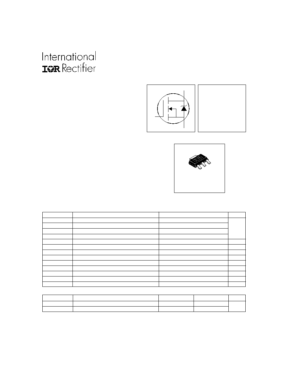
IRFL024N
HEXFET
®
Power MOSFET
S
D
G
V
DSS
= 55V
R
DS(on)
= 0.075
I
D
= 2.8A
Fifth Generation HEXFETs from International Rectifier
utilize advanced processing techniques to achieve
extremely low on-resistance per silicon area. This benefit,
combined with the fast switching speed and ruggedized
device design that HEXFET Power MOSFETs are well
known for, provides the designer with an extremely efficient
and reliable device for use in a wide variety of applications.
The SOT-223 package is designed for surface-mount
using vapor phase, infra red, or wave soldering techniques.
Its unique package design allows for easy automatic pick-
and-place as with other SOT or SOIC packages but has
the added advantage of improved thermal performance
due to an enlarged tab for heatsinking. Power dissipation
of 1.0W is possible in a typical surface mount application.
6/15/99
Description
l
Surface Mount
l
Advanced Process Technology
l
Ultra Low On-Resistance
l
Dynamic dv/dt Rating
l
Fast Switching
l
Fully Avalanche Rated
S O T -2 2 3
* When mounted on FR-4 board using minimum recommended footprint.
** When mounted on 1 inch square copper board, for comparison with other SMD devices.
Parameter
Typ.
Max.
Units
R
JA
Junction-to-Amb. (PCB Mount, steady state)*
90
120
R
JA
Junction-to-Amb. (PCB Mount, steady state)**
50
60
Thermal Resistance
°C/W
Parameter
Max.
Units
I
D
@ T
A
= 25°C
Continuous Drain Current, V
GS
@ 10V**
4.0
I
D
@ T
A
= 25°C
Continuous Drain Current, V
GS
@ 10V*
2.8
I
D
@ T
A
= 70°C
Continuous Drain Current, V
GS
@ 10V*
2.3
I
DM
Pulsed Drain Current
11.2
P
D
@T
A
= 25°C
Power Dissipation (PCB Mount)**
2.1
W
P
D
@T
A
= 25°C
Power Dissipation (PCB Mount)*
1.0
W
Linear Derating Factor (PCB Mount)*
8.3
mW/°C
V
GS
Gate-to-Source Voltage
± 20
V
E
AS
Single Pulse Avalanche Energy
214
mJ
I
AR
Avalanche Current
2.8
A
E
AR
Repetitive Avalanche Energy
*
0.1
mJ
dv/dt
Peak Diode Recovery dv/dt
5.0
V/ns
T
J,
T
STG
Junction and Storage Temperature Range
-55 to + 150
°C
Absolute Maximum Ratings
A
www.irf.com
1
PD - 91861A
IRFL024N
2
www.irf.com
Repetitive rating; pulse width limited by
max. junction temperature. ( See fig. 11 )
I
SD
1.68A, di/dt
155A/µs, V
DD
V
(BR)DSS
,
T
J
150°C
Notes:
Starting T
J
= 25°C, L = 54.7 mH
R
G
= 25
, I
AS
= 2.8A. (See Figure 12)
Pulse width
300µs; duty cycle
2%.
Parameter
Min. Typ. Max. Units
Conditions
I
S
Continuous Source Current
MOSFET symbol
(Body Diode)
showing the
I
SM
Pulsed Source Current
integral reverse
(Body Diode)
p-n junction diode.
V
SD
Diode Forward Voltage
1.0
V
T
J
= 25°C, I
S
=1.68A, V
GS
= 0V
t
rr
Reverse Recovery Time
35
53
ns
T
J
= 25°C, I
F
= 1.68A
Q
rr
Reverse RecoveryCharge
50
75
nC
di/dt = 100A/µs
t
on
Forward Turn-On Time
Intrinsic turn-on time is negligible (turn-on is dominated by L
S
+L
D
)
Source-Drain Ratings and Characteristics
11.2
2.8
A
Electrical Characteristics @ T
J
= 25°C (unless otherwise specified)
Parameter
Min. Typ. Max. Units
Conditions
V
(BR)DSS
Drain-to-Source Breakdown Voltage
55
V
V
GS
= 0V, I
D
= 250µA
V
(BR)DSS
/
T
J
Breakdown Voltage Temp. Coefficient
0.056
V/°C
Reference to 25°C, I
D
= 1mA
R
DS(on)
Static Drain-to-Source On-Resistance
0.075
V
GS
= 10V, I
D
= 2.8A
V
GS(th)
Gate Threshold Voltage
2.0
4.0
V
V
DS
= V
GS
, I
D
= 250µA
g
fs
Forward Transconductance
3.0
S
V
DS
= 25V, I
D
= 1.68A
25
µA
V
DS
= 55V, V
GS
= 0V
250
V
DS
= 44V, V
GS
= 0V, T
J
= 125°C
Gate-to-Source Forward Leakage
100
V
GS
= 20V
Gate-to-Source Reverse Leakage
-100
nA
V
GS
= -20V
Q
g
Total Gate Charge
18.3
I
D
= 1.68A
Q
gs
Gate-to-Source Charge
3.0
nC
V
DS
= 44V
Q
gd
Gate-to-Drain ("Miller") Charge
7.7
V
GS
= 10V, See Fig. 6 and 9
t
d(on)
Turn-On Delay Time
8.1
V
DD
= 28V
t
r
Rise Time
13.4
I
D
= 1.68A
t
d(off)
Turn-Off Delay Time
22.2
R
G
= 24
t
f
Fall Time
17.7
R
D
= 17
, See Fig. 10
C
iss
Input Capacitance
400
V
GS
= 0V
C
oss
Output Capacitance
145
pF
V
DS
= 25V
C
rss
Reverse Transfer Capacitance
60
= 1.0MHz, See Fig. 5
I
GSS
ns
I
DSS
Drain-to-Source Leakage Current
IRFL024N
www.irf.com
3
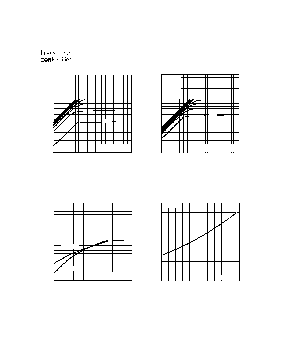
Fig 3. Typical Transfer Characteristics
Fig 4. Normalized On-Resistance
Vs. Temperature
Fig 1. Typical Output Characteristics,
Fig 2. Typical Output Characteristics,
1
10
100
4.5
5.0
5.5
6.0
6.5
V = 25V
20µs PULSE WIDTH
DS
V , Gate-to-Source Voltage (V)
I , Drain-to-Source Current (A)
GS
D
T = 150 C
J
°
T = 25 C
J
°
-60 -40 -20
0
20
40
60
80 100 120 140 160
0.0
0.5
1.0
1.5
2.0
T , Junction Temperature ( C)
R , Drain-to-Source On Resistance
(Normalized)
J
DS(on)
°
V
=
I =
GS
D
10V
2.8A
0.1
1
10
100
0.1
1
10
100
20µs PULSE WIDTH
T = 25 C
J
°
TOP
BOTTOM
VGS
15V
10V
8.0V
7.0V
6.0V
5.5V
5.0V
4.5V
V , Drain-to-Source Voltage (V)
I , Drain-to-Source Current (A)
DS
D
4.5V
0.1
1
10
100
0.1
1
10
100
20µs PULSE WIDTH
T = 150 C
J
°
TOP
BOTTOM
VGS
15V
10V
8.0V
7.0V
6.0V
5.5V
5.0V
4.5V
V , Drain-to-Source Voltage (V)
I , Drain-to-Source Current (A)
DS
D
4.5V
IRFL024N
4
www.irf.com
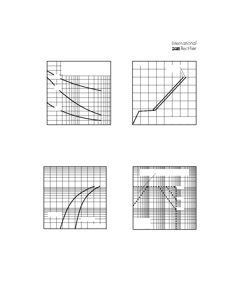
Fig 8. Maximum Safe Operating Area
Fig 6. Typical Gate Charge Vs.
Gate-to-Source Voltage
Fig 5. Typical Capacitance Vs.
Drain-to-Source Voltage
Fig 7. Typical Source-Drain Diode
Forward Voltage
1
10
100
0
100
200
300
400
500
600
700
V , Drain-to-Source Voltage (V)
C, Capacitance (pF)
DS
V
C
C
C
=
=
=
=
0V,
C
C
C
f = 1MHz
+ C
+ C
C SHORTED
GS
iss
gs
gd ,
ds
rss
gd
oss
ds
gd
C
iss
C
oss
C
rss
0.1
1
10
100
0.1
1
10
100
1000
OPERATION IN THIS AREA LIMITED
BY R
DS(on)
Single Pulse
T
T
= 150 C
= 25 C
°
°
J
C
V , Drain-to-Source Voltage (V)
I , Drain Current (A)
I , Drain Current (A)
DS
D
100us
1ms
10ms
0
5
10
15
20
0
5
10
15
20
Q , Total Gate Charge (nC)
V , Gate-to-Source Voltage (V)
G
GS
FOR TEST CIRCUIT
SEE FIGURE
I =
D
13
1.68 A
V
= 27V
DS
V
= 44V
DS
0.1
1
10
100
0.2
0.4
0.6
0.8
1.0
1.2
V ,Source-to-Drain Voltage (V)
I , Reverse Drain Current (A)
SD
SD
V = 0 V
GS
T = 25 C
J
°
T = 150 C
J
°
IRFL024N
www.irf.com
5
Q
G
Q
GS
Q
GD
V
G
Charge
+
-
V
DS
10V
Pulse Width
1
µs
Duty Factor
0.1 %
R
D
V
GS
V
DD
R
G
D.U.T.
D.U.T.
V
DS
I
D
I
G
3mA
V
GS
.3
µ
F
50K
.2
µ
F
12V
Current Regulator
Same Type as D.U.T.
Current Sampling Resistors
+
-
V
DS
90%
10%
V
GS
t
d(on)
t
r
t
d(off)
t
f
Fig 10b. Switching Time Waveforms
Fig 10a. Switching Time Test Circuit
Fig 9a. Basic Gate Charge Waveform
Fig 9b. Gate Charge Test Circuit
Fig 11. Maximum Effective Transient Thermal Impedance, Junction-to-Ambient
10V
0.1
1
10
100
1000
0.0001
0.001
0.01
0.1
1
10
100
1000
Notes:
1. Duty factor D = t / t
2. Peak T = P
x Z
+ T
1
2
J
DM
thJC
C
P
t
t
DM
1
2
t , Rectangular Pulse Duration (sec)
Thermal Response
(Z )
1
thJC
0.01
0.02
0.05
0.10
0.20
D = 0.50
SINGLE PULSE
(THERMAL RESPONSE)
IRFL024N
6
www.irf.com
Fig 12c. Maximum Avalanche Energy
Vs. Drain Current
Fig 12b. Unclamped Inductive Waveforms
tp
V
(B R )D SS
I
A S
Fig 12a. Unclamped Inductive Test Circuit
R G
IA S
0 .0 1
tp
D .U .T
L
V D S
+
-
VD D
D R IV E R
A
1 5V
1 0 V
25
50
75
100
125
150
0
100
200
300
400
500
Starting T , Junction Temperature ( C)
E , Single Pulse Avalanche Energy (mJ)
J
AS
°
ID
TOP
BOTTOM
1.3A
2.2A
2.8A
IRFL024N
www.irf.com
7
Package Outline
SOT-223 (TO-261AA) Outline
SOT-223
Part Marking Information
D A TE CO D E (Y W W )
Y = LA S T D IG IT O F TH E Y E A R
W W = W E E K
B O TT O M
P A R T NU M B E R
T O P
IN TE RN A TIO NA L
RE CT IF IE R
LO G O
E X A M P L E : T H IS IS A N IR FL 0 14
W A F E R
LO T CO D E
X X X X X X
31 4
F L0 14
IRFL024N
8
www.irf.com
SOT-223 Outline
Tape & Reel Information
4 .1 0 (.1 6 1 )
3 .9 0 (.1 5 4 )
1 .8 5 (.0 7 2 )
1 .6 5 (.0 6 5 )
2 .0 5 ( .0 8 0 )
1 .9 5 ( .0 7 7 )
1 2 .1 0 ( .4 7 5 )
1 1 .9 0 ( .4 6 9 )
7 .1 0 ( .2 7 9 )
6 .9 0 ( .2 7 2 )
1 .6 0 ( .0 6 2 )
1 .5 0 ( .0 5 9 )
T Y P .
7 .5 5 (.2 9 7)
7 .4 5 (.2 9 4)
7 .6 0 ( .2 9 9 )
7 .4 0 ( .2 9 2 )
2 .3 0 ( .0 9 0 )
2 .1 0 ( .0 8 3 )
1 6 .3 0 ( .6 4 1 )
1 5 .7 0 ( .6 1 9 )
0 .3 5 (.0 1 3 )
0 .2 5 (.0 1 0 )
F E E D D IR E C T IO N
T R
1 3 . 2 0 (.5 1 9 )
1 2 . 8 0 (.5 0 4 )
5 0. 00 ( 1 .9 6 9 )
M IN .
330.00
(13.000)
M A X .
N O T E S :
1 . C O N T R O L L I N G D IM E N S I O N : M IL L IM E T E R .
2 . O U T L IN E C O N F O R M S T O E IA -4 8 1 & E IA -5 4 1 .
3 . E A C H O 3 30 . 0 0 (1 3 .0 0 ) R E E L C O N T A I N S 2 ,5 0 0 D E V I C E S .
3
N O T E S :
1 . O U T LIN E C O M F O R M S T O E IA -4 1 8 - 1 .
2 . C O N T R O L L IN G D IM E N S IO N : M IL L IM E T E R . .
3 . D IM E N S IO N M E A S U R E D @ H U B .
4 . IN C L U D E S F L A N G E D IS T O R T IO N @ O U T E R E D G E .
1 5 .40 ( .6 0 7)
1 1 .90 ( .4 6 9)
1 8 .4 0 (. 72 4 )
M A X .
1 4 .4 0 (. 5 6 6 )
1 2 .4 0 (. 4 8 8 )
4
4
WORLD HEADQUARTERS: 233 Kansas St., El Segundo, California 90245, Tel: (310) 322 3331
IR GREAT BRITAIN: Hurst Green, Oxted, Surrey RH8 9BB, UK Tel: ++ 44 1883 732020
IR CANADA: 15 Lincoln Court, Brampton, Ontario L6T3Z2, Tel: (905) 453 2200
IR GERMANY: Saalburgstrasse 157, 61350 Bad Homburg Tel: ++ 49 6172 96590
IR ITALY: Via Liguria 49, 10071 Borgaro, Torino Tel: ++ 39 11 451 0111
IR FAR EAST: K&H Bldg., 2F, 30-4 Nishi-Ikebukuro 3-Chome, Toshima-Ku, Tokyo Japan 171 Tel: 81 3 3983 0086
IR SOUTHEAST ASIA: 1 Kim Seng Promenade, Great World City West Tower, 13-11, Singapore 237994 Tel: ++ 65 838 4630
IR TAIWAN:16 Fl. Suite D. 207, Sec. 2, Tun Haw South Road, Taipei, 10673, Taiwan Tel: 886-2-2377-9936
http://www.irf.com/ Data and specifications subject to change without notice. 6/99