Äîêóìåíòàöèÿ è îïèñàíèÿ www.docs.chipfind.ru
IRFP32N50K
05/24/01
www.irf.com
1
SMPS MOSFET
HEXFET
®
Power MOSFET
V
DSS
R
DS(on)
typ.
I
D
500V
0.135
32A
Parameter
Max.
Units
I
D
@ T
C
= 25°C
Continuous Drain Current, V
GS
@ 10V
32
I
D
@ T
C
= 100°C
Continuous Drain Current, V
GS
@ 10V
20
A
I
DM
Pulsed Drain Current
130
P
D
@T
C
= 25°C
Power Dissipation
460
W
Linear Derating Factor
3.7
W/°C
V
GS
Gate-to-Source Voltage
± 30
V
dv/dt
Peak Diode Recovery dv/dt
13
V/ns
T
J
Operating Junction and
-55 to + 150
T
STG
Storage Temperature Range
Soldering Temperature, for 10 seconds
300
(1.6mm from case )
°C
Mounting torque, 6-32 or M3 screw
10lb*in (1.1N*m)
Absolute Maximum Ratings
TO-247AC
Symbol
Parameter
Typ.
Max.
Units
E
AS
Single Pulse Avalanche Energy
450
mJ
I
AR
Avalanche Current
32
A
E
AR
Repetitive Avalanche Energy
46
mJ
Symbol
Parameter
Typ.
Max.
Units
R
JC
Junction-to-Case
0.26
R
CS
Case-to-Sink, Flat, Greased Surface
0.24
°C/W
R
JA
Junction-to-Ambient
40
Thermal Resistance
Avalanche Characteristics
l
Switch Mode Power Supply (SMPS)
l
Uninterruptible Power Supply
l
High Speed Power Switching
l
Hard Switched and High Frequency
Circuits
Benefits
Applications
l
Low Gate Charge Qg results in Simple
Drive Requirement
l
Improved Gate, Avalanche and Dynamic
dv/dt Ruggedness
l
Fully Characterized Capacitance and
Avalanche Voltage and Current
l
Low R
DS(on)
PD - 94099A
IRFP32N50K
2
www.irf.com
Symbol
Parameter
Min. Typ. Max. Units
Conditions
V
(BR)DSS
Drain-to-Source Breakdown Voltage
500
V
V
GS
= 0V, I
D
= 250µA
V
(BR)DSS
/
T
J
Breakdown Voltage Temp. Coefficient
0.54
V/°C
Reference to 25°C, I
D
= 1mA
R
DS(on)
Static Drain-to-Source On-Resistance
0.135 0.16
V
GS
= 10V, I
D
= 32A
V
GS(th)
Gate Threshold Voltage
3.0
5.0
V
V
DS
= V
GS
, I
D
= 250µA
50
µA
V
DS
= 500V, V
GS
= 0V
250
µA
V
DS
= 400V, V
GS
= 0V, T
J
= 150°C
Gate-to-Source Forward Leakage
100
V
GS
= 30V
Gate-to-Source Reverse Leakage
-100
nA
V
GS
= -30V
Static @ T
J
= 25°C (unless otherwise specified)
I
GSS
I
DSS
Drain-to-Source Leakage Current
Repetitive rating; pulse width limited by
max. junction temperature.
I
SD
32A, di/dt
197A/µs, V
DD
V
(BR)DSS
,
T
J
150°C
Notes:
Starting T
J
= 25°C, L = 0.87mH, R
G
= 25
,
I
AS
= 32A,
Pulse width
400µs; duty cycle
2%.
Parameter
Min. Typ. Max. Units
Conditions
g
fs
Forward Transconductance
14
S
V
DS
= 50V, I
D
= 32A
Q
g
Total Gate Charge
190 I
D
= 32A
Q
gs
Gate-to-Source Charge
59
nC
V
DS
= 400V
Q
gd
Gate-to-Drain ("Miller") Charge
84
V
GS
= 10V
t
d(on)
Turn-On Delay Time
28
V
DD
= 250V
t
r
Rise Time
120
I
D
= 32A
t
d(off)
Turn-Off Delay Time
48
R
G
= 4.3
t
f
Fall Time
54
V
GS
= 10V
C
iss
Input Capacitance
5280
V
GS
= 0V
C
oss
Output Capacitance
550
V
DS
= 25V
C
rss
Reverse Transfer Capacitance
45
pF
= 1.0MHz, See Fig. 5
C
oss
Output Capacitance
5630
V
GS
= 0V, V
DS
= 1.0V, = 1.0MHz
C
oss
Output Capacitance
155
V
GS
= 0V, V
DS
= 400V, = 1.0MHz
C
oss
eff.
Effective Output Capacitance
265
V
GS
= 0V, V
DS
= 0V to 400V
Dynamic @ T
J
= 25°C (unless otherwise specified)
ns
Symbol
Parameter
Min. Typ. Max. Units
Conditions
I
S
Continuous Source Current
MOSFET symbol
(Body Diode)
showing the
I
SM
Pulsed Source Current
integral reverse
(Body Diode)
p-n junction diode.
V
SD
Diode Forward Voltage
1.5
V
T
J
= 25°C, I
S
= 32A, V
GS
= 0V
t
rr
Reverse Recovery Time
530
800
ns
T
J
= 25°C, I
F
= 32A
Q
rr
Reverse RecoveryCharge
9.0
13.5
µC
di/dt = 100A/µs
I
RRM
Reverse RecoveryCurrent
30
A
t
on
Forward Turn-On Time
Intrinsic turn-on time is negligible (turn-on is dominated by L
S
+L
D
)
S
D
G
Diode Characteristics
32
130
A
C
oss
eff. is a fixed capacitance that gives the same charging time
as C
oss
while V
DS
is rising from 0 to 80% V
DSS
.
IRFP32N50K
www.irf.com
3
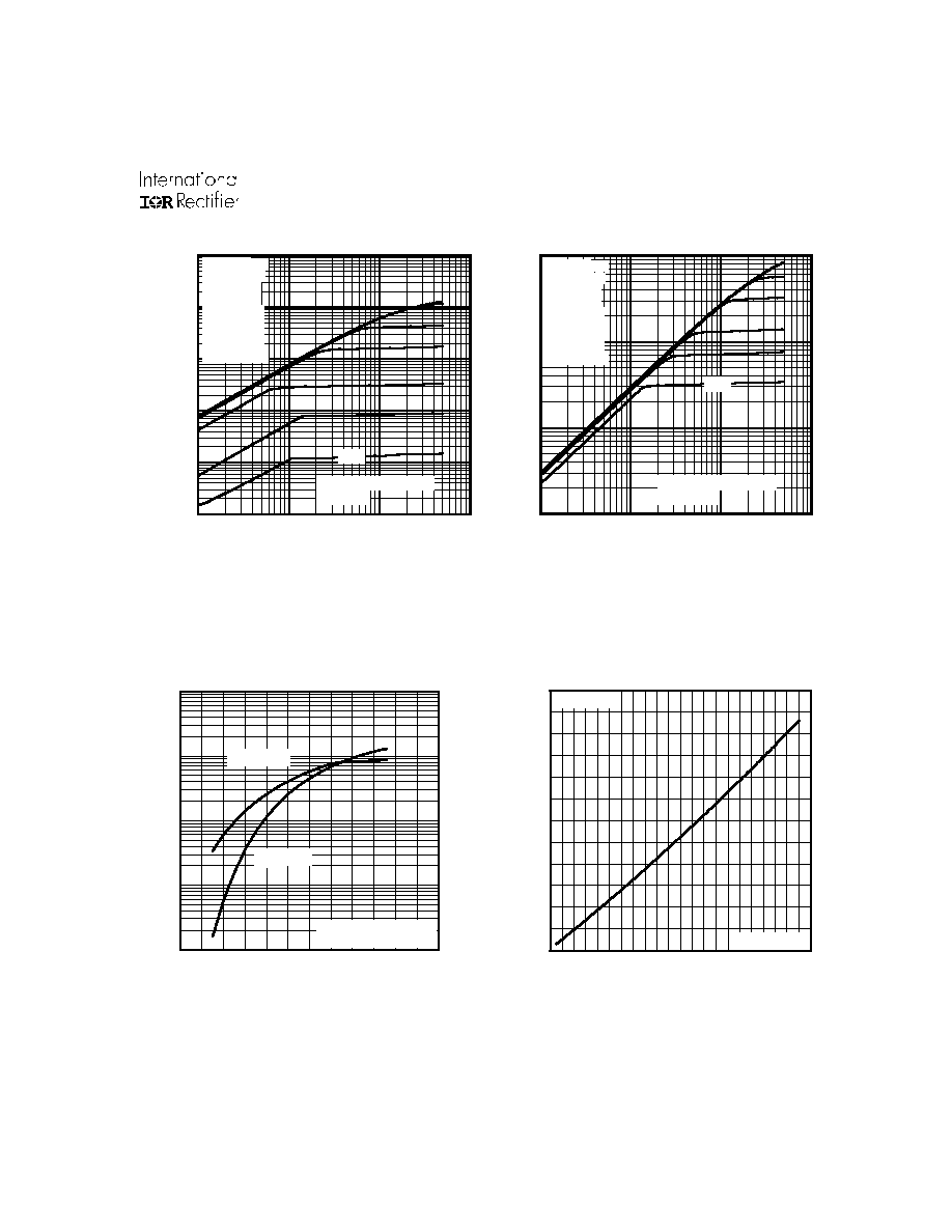
Fig 4. Normalized On-Resistance
Vs. Temperature
Fig 2. Typical Output Characteristics
Fig 1. Typical Output Characteristics
Fig 3. Typical Transfer Characteristics
0.1
1
10
100
VDS, Drain-to-Source Voltage (V)
0.01
0.1
1
10
100
1000
I D
, Drain-to-Source Current (A)
5.0V
20µs PULSE WIDTH
Tj = 25°C
VGS
TOP 15V
12V
10V
8.0V
7.0V
6.0V
5.5V
BOTTOM 5.0V
0.1
1
10
100
VDS, Drain-to-Source Voltage (V)
0.1
1
10
100
I D
, Drain-to-Source Current (A)
5.0V
20µs PULSE WIDTH
Tj = 150°C
VGS
TOP 15V
12V
10V
8.0V
7.0V
6.0V
5.5V
BOTTOM 5.0V
0.1
1
10
100
1000
4
5
7
8
9
11
12
V = 50V
20µs PULSE WIDTH
DS
V , Gate-to-Source Voltage (V)
I , Drain-to-Source Current (A)
GS
D
T = 150 C
J
°
T = 25 C
J
°
-60 -40 -20
0
20
40
60
80 100 120 140 160
0.0
0.5
1.0
1.5
2.0
2.5
3.0
T , Junction Temperature ( C)
R , Drain-to-Source On Resistance
(Normalized)
J
DS(on)
°
V
=
I =
GS
D
10V
32A
IRFP32N50K
4
www.irf.com
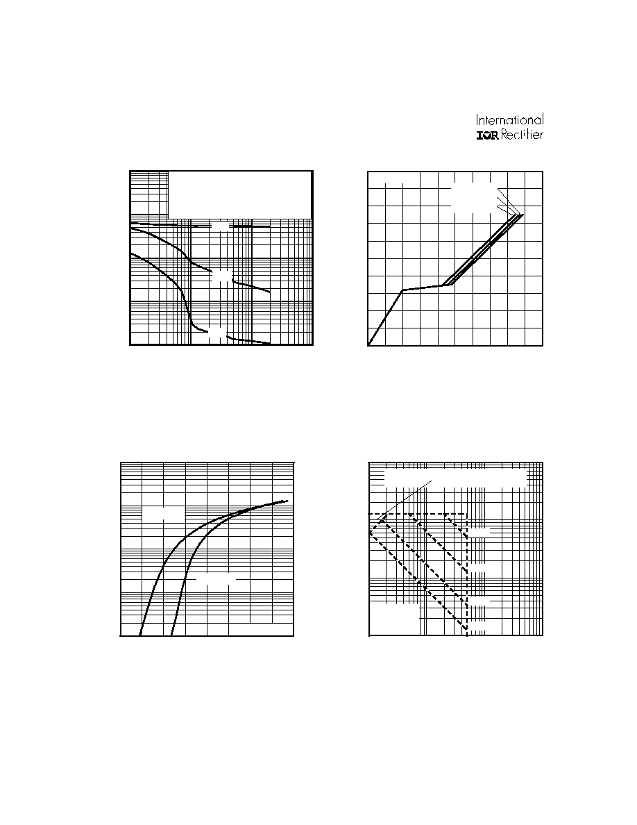
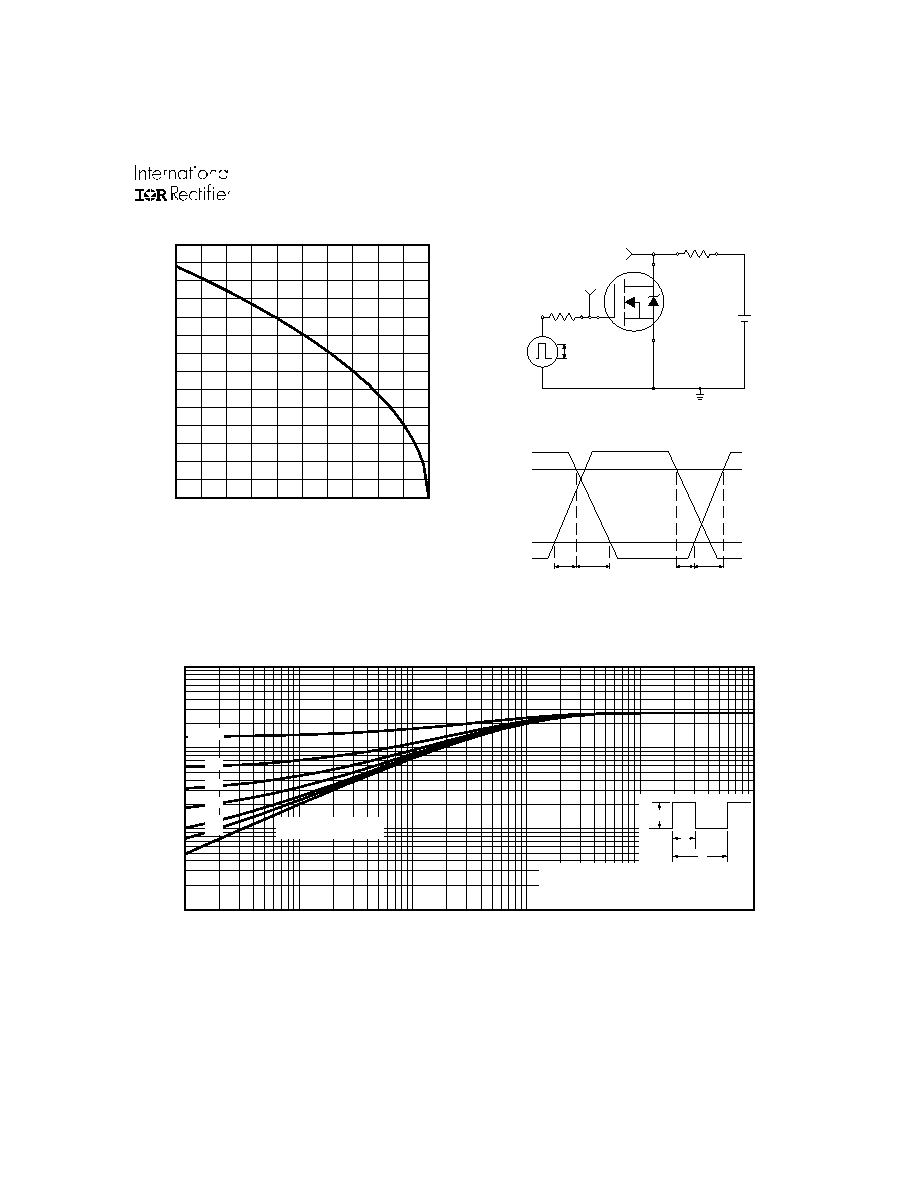
Fig 8. Maximum Safe Operating Area
Fig 6. Typical Gate Charge Vs.
Gate-to-Source Voltage
Fig 5. Typical Capacitance Vs.
Drain-to-Source Voltage
Fig 7. Typical Source-Drain Diode
Forward Voltage
1
10
100
1000
VDS, Drain-to-Source Voltage (V)
10
100
1000
10000
100000
C, Capacitance(pF)
Coss
Crss
Ciss
VGS = 0V, f = 1 MHZ
Ciss = Cgs + Cgd, Cds SHORTED
Crss = Cgd
Coss = Cds + Cgd
0
40
80
120
160
200
0
4
8
12
16
20
Q , Total Gate Charge (nC)
V , Gate-to-Source Voltage (V)
G
GS
I =
D
32A
V
= 100V
DS
V
= 250V
DS
V
= 400V
DS
0.1
1
10
100
1000
0.2
0.6
0.9
1.3
1.6
V ,Source-to-Drain Voltage (V)
I , Reverse Drain Current (A)
SD
SD
V = 0 V
GS
T = 150 C
J
°
T = 25 C
J
°
1
10
100
1000
10
100
1000
10000
OPERATION IN THIS AREA LIMITED
BY R
DS(on)
Single Pulse
T
T
= 150 C
= 25 C
°
°
J
C
V , Drain-to-Source Voltage (V)
I , Drain Current (A)
I , Drain Current (A)
DS
D
10us
100us
1ms
10ms
IRFP32N50K
www.irf.com
5
Fig 10a. Switching Time Test Circuit
V
DS
90%
10%
V
GS
t
d(on)
t
r
t
d(off)
t
f
Fig 10b. Switching Time Waveforms
V
DS
Pulse Width
1
µs
Duty Factor
0.1 %
R
D
V
GS
R
G
D.U.T.
10V
+
-
V
DD
Fig 11. Maximum Effective Transient Thermal Impedance, Junction-to-Case
Fig 9. Maximum Drain Current Vs.
Case Temperature
25
50
75
100
125
150
0
5
10
15
20
25
30
35
T , Case Temperature ( C)
I , Drain Current (A)
°
C
D
0.001
0.01
0.1
1
0.00001
0.0001
0.001
0.01
0.1
1
Notes:
1. Duty factor D = t / t
2. Peak T = P
x Z
+ T
1
2
J
DM
thJC
C
P
t
t
DM
1
2
t , Rectangular Pulse Duration (sec)
Thermal Response
(Z )
1
thJC
0.01
0.02
0.05
0.10
0.20
D = 0.50
SINGLE PULSE
(THERMAL RESPONSE)