 | ÐлекÑÑоннÑй компоненÑ: IRFP460P | СкаÑаÑÑ:  PDF PDF  ZIP ZIP |
Äîêóìåíòàöèÿ è îïèñàíèÿ www.docs.chipfind.ru
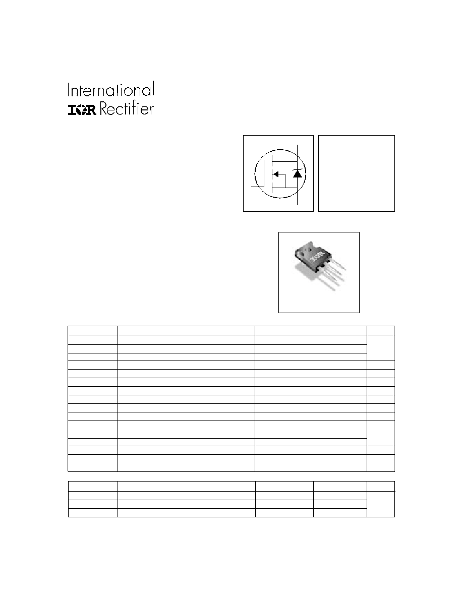
IRFP460P
HEXFET
®
Power MOSFET
Third Generation HEXFET
®
s from International Rectifier
provide the designer with the best combination of fast
switching, ruggedized device design, low on-resistance
and cost-effectiveness.
The TO-247 package is preferred for commercial-industrial
applications where higher power levels preclude the use
of TO-220 devices. The TO-247 is similar but superior to
the earlier TO-218 package because of its isolated
mounting hole. It also provides greater creepage distance
between pins to meet the requirements of most safety
specifications.
The solder plated version of the TO-247 allows the reflow
soldering of the package heatsink to a substrate material.
S
D
G
V
DSS
= 500V
R
DS(on)
= 0.27
I
D
= 20A
l
Dynamic dv/dt Rating
l
Repetitive Avalanche Rated
l
Isolated Central Mounting Hole
l
Fast Switching
l
Ease of Paralleling
Description
Parameter
Max.
Units
I
D
@ T
C
= 25°C
Continuous Drain Current, V
GS
@ 10V
20
I
D
@ T
C
= 100°C
Continuous Drain Current, V
GS
@ 10V
13
A
I
DM
Pulsed Drain Current
80
P
D
@T
C
= 25°C
Power Dissipation
280
W
Linear Derating Factor
2.2
W/°C
V
GS
Gate-to-Source Voltage
± 20
V
E
AS
Single Pulse Avalanche Energy
960
mJ
I
AR
Avalanche Current
20
A
E
AR
Repetitive Avalanche Energy
28
mJ
dv/dt
Peak Diode Recovery dv/dt
3.5
V/ns
T
J
Operating Junction and
-55 to + 150
T
STG
Storage Temperature Range
Soldering Temperature, for 10 seconds
300 (1.6mm from case )
°C
Mounting torque, 6-32 or M3 srew
10 lbf·in (1.1N·m)
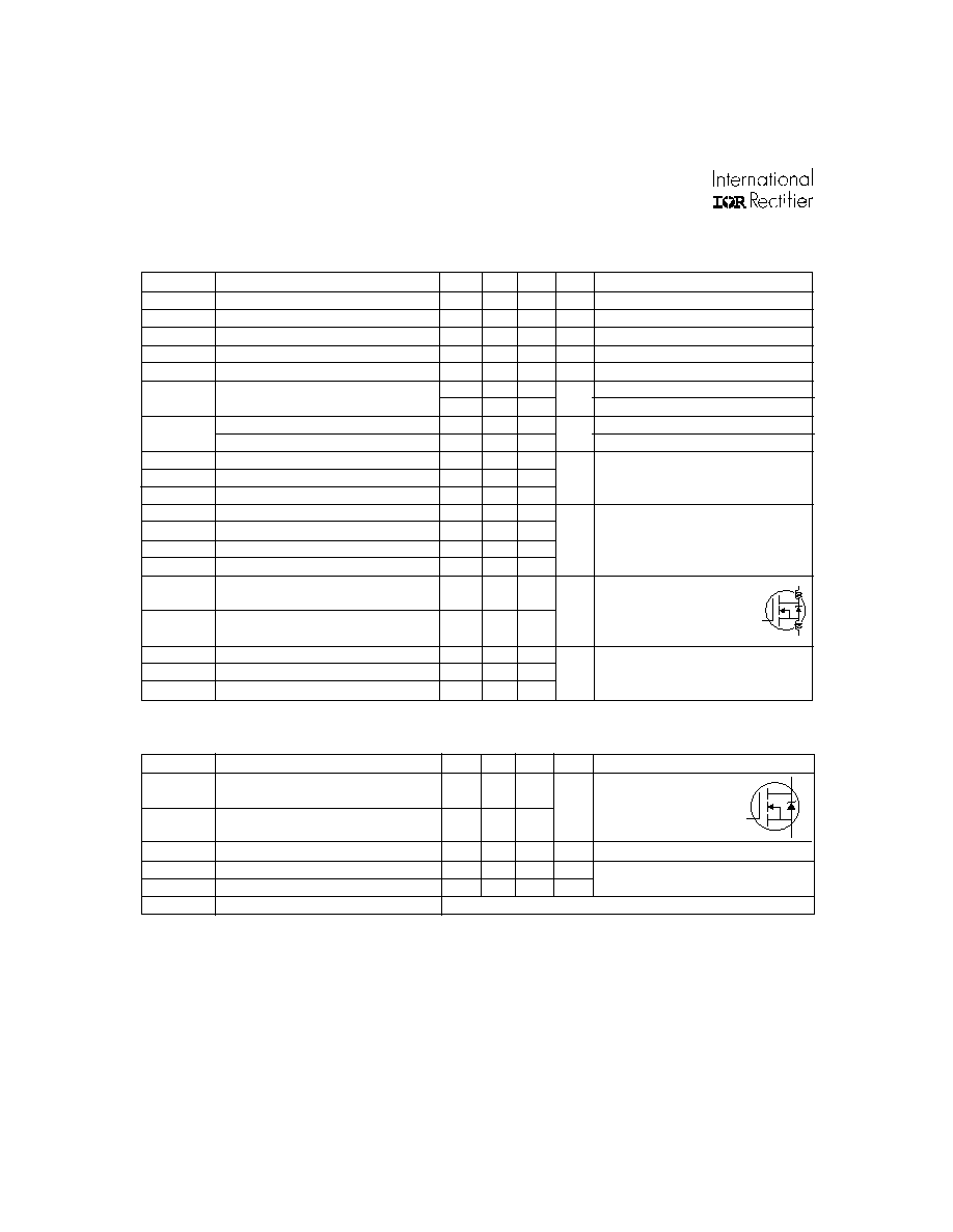
Absolute Maximum Ratings
Parameter
Typ.
Max.
Units
R
JC
Junction-to-Case
0.45
R
CS
Case-to-Sink, Flat, Greased Surface
0.24
°C/W
R
JA
Junction-to-Ambient
40
Thermal Resistance
01/17/01
www.irf.com
1
l
Simple Drive Requirements
l
Solder Plated for Reflowing
Maximum Reflow Temperature 230 (Time above 183 °C
should not exceed 100s) °C
TO-247AC
PD-93946A
2
www.irf.com
IRFP460P
Parameter
Min. Typ. Max. Units
Conditions
V
(BR)DSS
Drain-to-Source Breakdown Voltage
500
V
V
GS
= 0V, I
D
= 250µA
V
(BR)DSS
/
T
J
Breakdown Voltage Temp. Coefficient
0.63
V/°C
Reference to 25°C, I
D
= 1mA
R
DS(on)
Static Drain-to-Source On-Resistance
0.27
V
GS
= 10V, I
D
= 12A
V
GS(th)
Gate Threshold Voltage
2.0
4.0
V
V
DS
= V
GS
, I
D
= 250µA
g
fs
Forward Transconductance
13
S
V
DS
= 50V, I
D
=12A
25
µA
V
DS
= 500V, V
GS
= 0V
250
V
DS
= 400V, V
GS
= 0V, T
J
= 125°C
Gate-to-Source Forward Leakage
100
V
GS
= 20V
Gate-to-Source Reverse Leakage
-100
nA
V
GS
=-20V
Q
g
Total Gate Charge
210
I
D
= 20A
Q
gs
Gate-to-Source Charge
29
nC
V
DS
= 400V
Q
gd
Gate-to-Drain ("Miller") Charge
110
V
GS
= 10V, See Fig. 6 and 13
t
d(on)
Turn-On Delay Time
18
V
DD
= 250V
t
r
Rise Time
59
I
D
= 20A
t
d(off)
Turn-Off Delay Time
110
R
G
= 4.3
t
f
Fall Time
58
R
D
= 13
,See Fig. 10
Between lead,
6mm (0.25in.)
from package
and center of die contact
C
iss
Input Capacitance
4200
V
GS
= 0V
C
oss
Output Capacitance
870
V
DS
= 25V
C
rss
Reverse Transfer Capacitance
350
pF
= 1.0MHz, See Fig. 5
nH
Electrical Characteristics @ T
J
= 25°C (unless otherwise specified)
L
D
Internal Drain Inductance
L
S
Internal Source Inductance
S
D
G
I
GSS
ns
5.0
13
I
DSS
Drain-to-Source Leakage Current
Repetitive rating; pulse width limited by
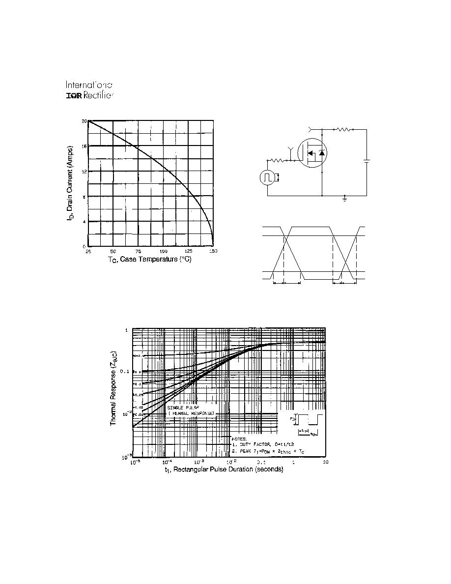
max. junction temperature. ( See fig. 11 )
I
SD
20A, di/dt
160A/µs, V
DD
V
(BR)DSS
,
T
J
150°C
Notes:
Starting T
J
= 25°C, L =4.8mH
R
G
= 25
, I
AS
= 20A. (See Figure 12)
Pulse width
300µs; duty cycle
2%.
S
D
G
Parameter
Min. Typ. Max. Units
Conditions
I
S
Continuous Source Current
MOSFET symbol
(Body Diode)
showing the
I
SM
Pulsed Source Current
integral reverse
(Body Diode)
p-n junction diode.
V
SD
Diode Forward Voltage
1.8
V
T
J
= 25°C, I
S
= 20A, V
GS
= 0V
t
rr
Reverse Recovery Time
570
860
ns
T
J
= 25°C, I
F
= 20A
Q
r r
Reverse RecoverCharge
5.7
8.6
µC
di/dt = 100A/µs
t
on
Forward Turn-On Time
Intrinsic turn-on time is negligible (turn-on is dominated by L
S
+L
D
)
Source-Drain Ratings and Characteristics
20
80
A
www.irf.com
3
IRFP460P
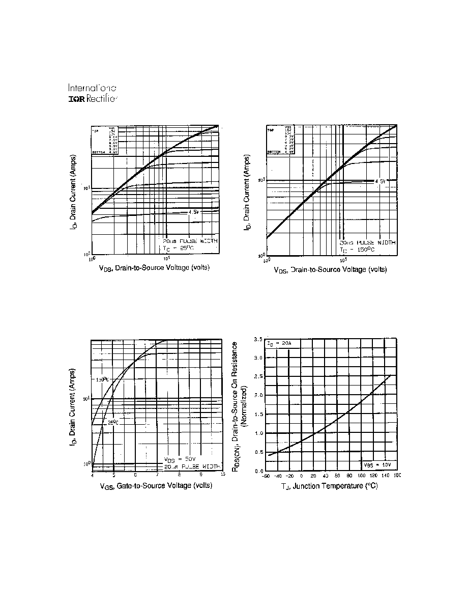
Fig 1. Typical Output Characteristics
Fig 3. Typical Transfer Characteristics
Fig 4. Normalized On-Resistance
Vs. Temperature
Fig 2. Typical Output Characteristics
4
www.irf.com
IRFP460P
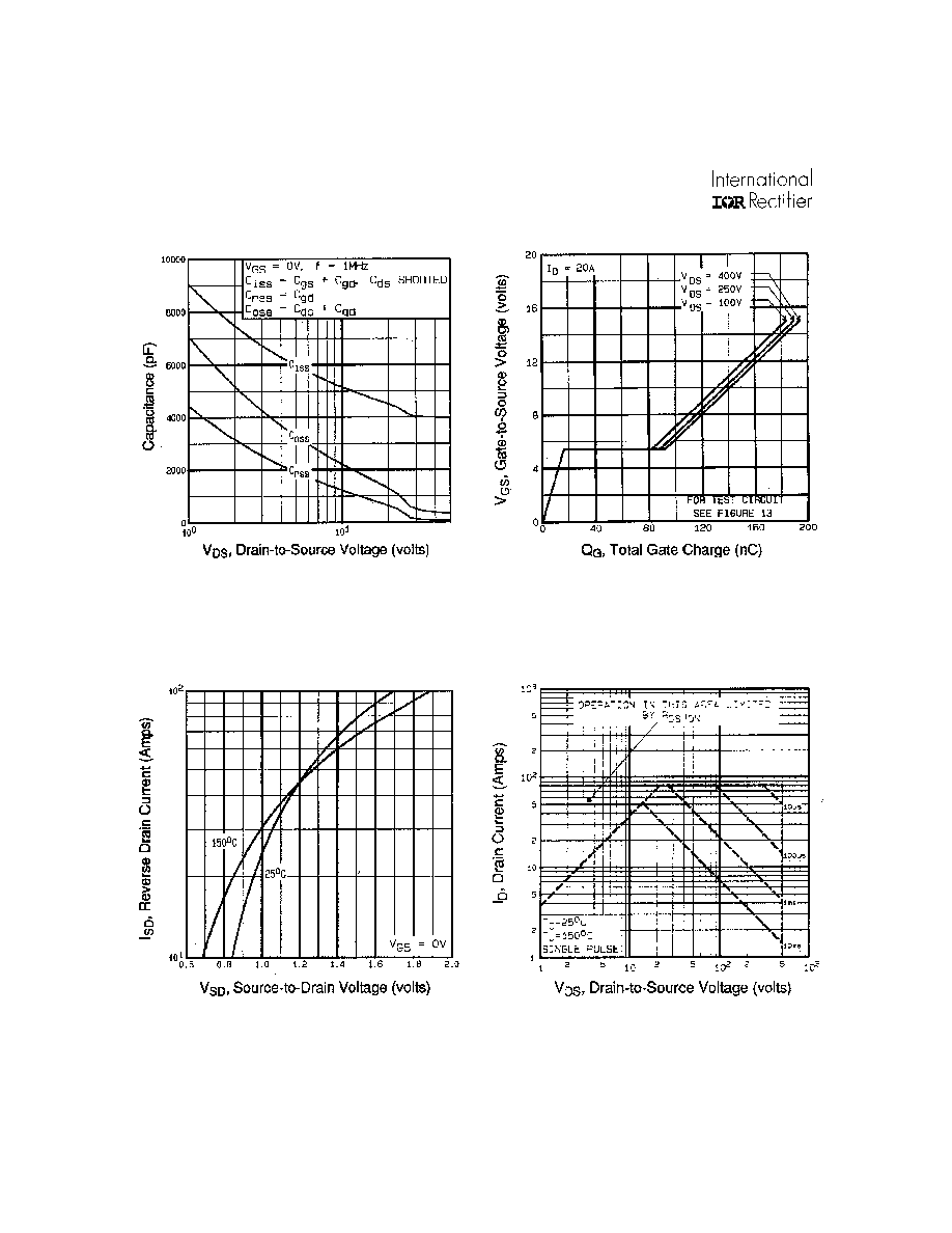
Fig 8. Maximum Safe Operating Area
Fig 6. Typical Gate Charge Vs.
Gate-to-Source Voltage
Fig 5. Typical Capacitance Vs.
Drain-to-Source Voltage
Fig 7. Typical Source-Drain Diode
Forward Voltage
www.irf.com
5
IRFP460P
Fig 9. Maximum Drain Current Vs.
Case Temperature
Fig 10a. Switching Time Test Circuit
V
DS
90%
10%
V
GS
t
d(on)
t
r
t
d(off)
t
f
Fig 10b. Switching Time Waveforms
V
DS
Pulse Width
1
µs
Duty Factor
0.1 %
R
D
V
GS
R
G
D.U.T.
10V
+
-
V
DD
Fig 11. Maximum Effective Transient Thermal Impedance, Junction-to-Case