Parameter
Max.
Units
I
D
@ T
C
= 25∞C
Continuous Drain Current, V
GS
@ 10V
31
I
D
@ T
C
= 100∞C
Continuous Drain Current, V
GS
@ 10V
21
A
I
DM
Pulsed Drain Current
124
P
D
@T
A
= 25∞C
Power Dissipation
3.1
W
P
D
@T
C
= 25∞C
Power Dissipation
200
Linear Derating Factor
1.3
W/∞C
V
GS
Gate-to-Source Voltage
± 30
V
dv/dt
Peak Diode Recovery dv/dt
2.1
V/ns
T
J
Operating Junction and
-55 to + 175
T
STG
Storage Temperature Range
Soldering Temperature, for 10 seconds
300 (1.6mm from case )
∞C
Mounting torqe, 6-32 or M3 screw
10 lbf∑in (1.1N∑m)
www.irf.com
1
2/14/00
IRFB31N20D
IRFS31N20D
IRFSL31N20D
SMPS MOSFET
HEXFET
Æ
Power MOSFET
l
High frequency DC-DC converters
Benefits
Applications
l
Low Gate-to-Drain Charge to Reduce
Switching Losses
l
Fully Characterized Capacitance Including
Effective C
OSS
to Simplify Design, (See
App. Note AN1001)
l
Fully Characterized Avalanche Voltage
and Current
V
DSS
R
DS(on)
max
I
D
200V
0.082
31A
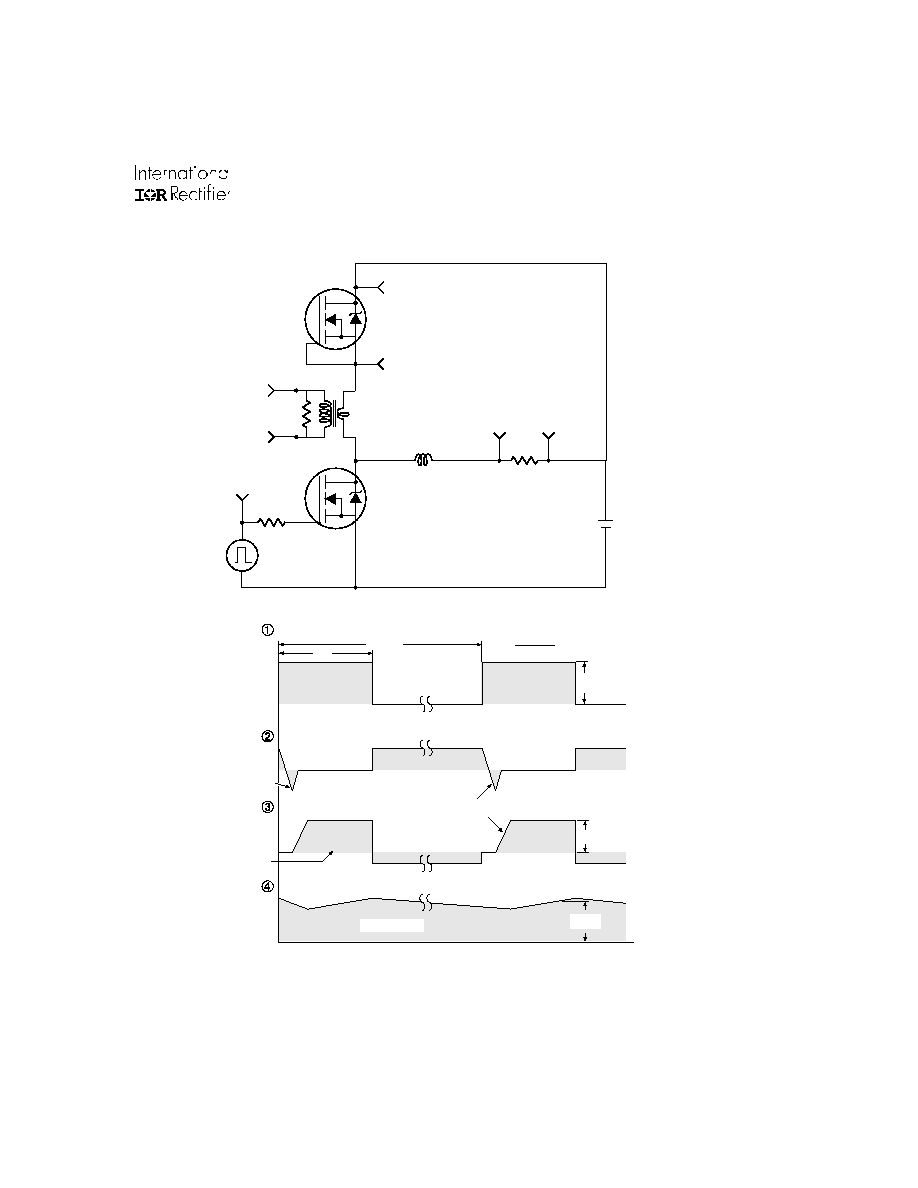
Typical SMPS Topologies
l
Telecom 48V Input Forward Converters
Absolute Maximum Ratings
Notes
through
are on page 11
D
2
Pak
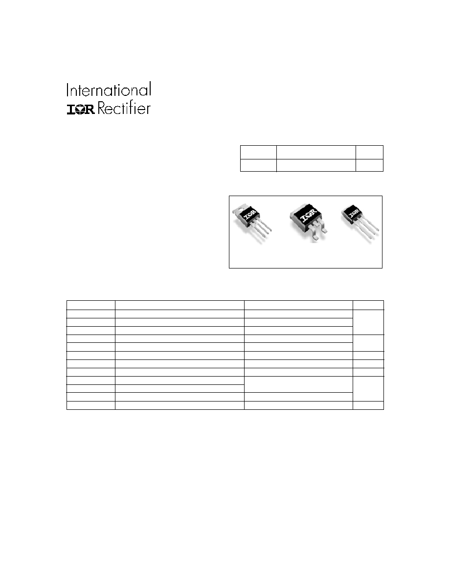
IRFS31N20D
TO-220AB
IRFB31N20D
TO-262
IRFSL31N20D
PD- 93805B
IRFB/IRFS/IRFSL31N20D
2
www.irf.com
Parameter
Min. Typ. Max. Units
Conditions
g
fs
Forward Transconductance
17
≠≠≠
≠≠≠
S
V
DS
= 50V, I
D
= 18A
Q
g
Total Gate Charge
≠≠≠
70
110 I
D
= 18A
Q
gs
Gate-to-Source Charge
≠≠≠
18
27
nC
V
DS
= 160V
Q
gd
Gate-to-Drain ("Miller") Charge
≠≠≠
33
49
V
GS
= 10V,
t
d(on)
Turn-On Delay Time
≠≠≠
16
≠≠≠
V
DD
= 100V
t
r
Rise Time
≠≠≠
38
≠≠≠
I
D
= 18A
t
d(off)
Turn-Off Delay Time
≠≠≠
26
≠≠≠
R
G
= 2.5
t
f
Fall Time
≠≠≠
10
≠≠≠
R
D
= 5.4
C
iss
Input Capacitance
≠≠≠
2370 ≠≠≠
V
GS
= 0V
C
oss
Output Capacitance
≠≠≠
390
≠≠≠
V
DS
= 25V
C
rss
Reverse Transfer Capacitance
≠≠≠
78
≠≠≠
pF
= 1.0MHz
C
oss
Output Capacitance
≠≠≠
2860 ≠≠≠
V
GS
= 0V, V
DS
= 1.0V, = 1.0MHz
C
oss
Output Capacitance
≠≠≠
150
≠≠≠
V
GS
= 0V, V
DS
= 160V, = 1.0MHz
C
oss
eff.
Effective Output Capacitance
≠≠≠
170
≠≠≠
V
GS
= 0V, V
DS
= 0V to 160V
Dynamic @ T
J
= 25∞C (unless otherwise specified)
ns
Parameter
Typ.
Max.
Units
E
AS
Single Pulse Avalanche Energy
≠≠≠
420
mJ
I
AR
Avalanche Current
≠≠≠
18
A
E
AR
Repetitive Avalanche Energy
≠≠≠
20
mJ
Avalanche Characteristics
S
D
G
Parameter
Min. Typ. Max. Units
Conditions
I
S
Continuous Source Current
MOSFET symbol
(Body Diode)
≠≠≠
≠≠≠
showing the
I
SM
Pulsed Source Current
integral reverse
(Body Diode)
≠≠≠
≠≠≠
p-n junction diode.
V
SD
Diode Forward Voltage
≠≠≠
≠≠≠
1.3
V
T
J
= 25∞C, I
S
= 18A, V
GS
= 0V
t
rr
Reverse Recovery Time
≠≠≠
200
300
ns
T
J
= 25∞C, I
F
= 18A
Q
rr
Reverse RecoveryCharge
≠≠≠
1.7
2.6
µC
di/dt = 100A/µs
t
on
Forward Turn-On Time
Intrinsic turn-on time is negligible (turn-on is dominated by L
S
+L
D
)
Diode Characteristics
31
124
A
Static @ T
J
= 25∞C (unless otherwise specified)
Parameter
Min. Typ. Max. Units
Conditions
V
(BR)DSS
Drain-to-Source Breakdown Voltage
200
≠≠≠
≠≠≠
V
V
GS
= 0V, I
D
= 250µA
V
(BR)DSS
/
T
J
Breakdown Voltage Temp. Coefficient
≠≠≠ 0.25 ≠≠≠ V/∞C Reference to 25∞C, I
D
= 1mA
R
DS(on)
Static Drain-to-Source On-Resistance
≠≠≠
≠≠≠ 0.082
V
GS
= 10V, I
D
= 18A
V
GS(th)
Gate Threshold Voltage
3.0
≠≠≠
5.5
V
V
DS
= V
GS
, I
D
= 250µA
≠≠≠
≠≠≠
25
µA
V
DS
= 200V, V
GS
= 0V
≠≠≠
≠≠≠
250
V
DS
= 160V, V
GS
= 0V, T
J
= 150∞C
Gate-to-Source Forward Leakage
≠≠≠
≠≠≠
100
V
GS
= 30V
Gate-to-Source Reverse Leakage
≠≠≠
≠≠≠
-100
nA
V
GS
= -30V
I
GSS
I
DSS
Drain-to-Source Leakage Current
Thermal Resistance
Parameter
Typ.
Max.
Units
R
JC
Junction-to-Case
≠≠≠
0.75
R
CS
Case-to-Sink, Flat, Greased Surface
0.50
≠≠≠
∞C/W
R
JA
Junction-to-Ambient
≠≠≠
62
R
JA
Junction-to-Ambient
≠≠≠
40
IRFB/IRFS/IRFSL31N20D
www.irf.com
3
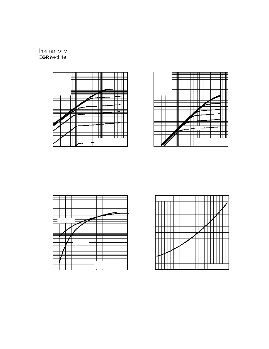
Fig 4. Normalized On-Resistance
Vs. Temperature
Fig 2. Typical Output Characteristics
Fig 1. Typical Output Characteristics
Fig 3. Typical Transfer Characteristics
0.1
1
10
100
1000
0.1
1
10
100
20µs PULSE WIDTH
T = 25 C
J
∞
TOP
BOTTOM
VGS
15V
12V
10V
8.0V
7.0V
6.5V
6.0V
5.5V
V , Drain-to-Source Voltage (V)
I , Drain-to-Source Current (A)
DS
D
5.5V
1
10
100
1000
0.1
1
10
100
20µs PULSE WIDTH
T = 175 C
J
∞
TOP
BOTTOM
VGS
15V
12V
10V
8.0V
7.0V
6.5V
6.0V
5.5V
V , Drain-to-Source Voltage (V)
I , Drain-to-Source Current (A)
DS
D
5.5V
0.1
1
10
100
1000
5
6
7
8
9
10
11
V = 50V
20µs PULSE WIDTH
DS
V , Gate-to-Source Voltage (V)
I , Drain-to-Source Current (A)
GS
D
T = 25 C
J
∞
T = 175 C
J
∞
-60 -40 -20
0
20 40 60 80 100 120 140 160 180
0.0
0.5
1.0
1.5
2.0
2.5
3.0
T , Junction Temperature ( C)
R , Drain-to-Source On Resistance
(Normalized)
J
DS(on)
∞
V
=
I =
GS
D
10V
30A

IRFB/IRFS/IRFSL31N20D
4
www.irf.com
Fig 8. Maximum Safe Operating Area
Fig 6. Typical Gate Charge Vs.
Gate-to-Source Voltage
Fig 5. Typical Capacitance Vs.
Drain-to-Source Voltage
Fig 7. Typical Source-Drain Diode
Forward Voltage
0
20
40
60
80
100
0
4
8
12
16
20
Q , Total Gate Charge (nC)
V , Gate-to-Source Voltage (V)
G
GS
FOR TEST CIRCUIT
SEE FIGURE
I =
D
13
18A
V
= 40V
DS
V
= 100V
DS
V
= 160V
DS
0.1
1
10
100
1000
0.2
0.4
0.6
0.8
1.0
1.2
V ,Source-to-Drain Voltage (V)
I , Reverse Drain Current (A)
SD
SD
V = 0 V
GS
T = 25 C
J
∞
T = 175 C
J
∞
1
10
100
1000
1
10
100
1000
OPERATION IN THIS AREA LIMITED
BY R
DS(on)
Single Pulse
T
T
= 175 C
= 25 C
∞
∞
J
C
V , Drain-to-Source Voltage (V)
I , Drain Current (A)
I , Drain Current (A)
DS
D
10us
100us
1ms
10ms
1
10
100
1000
VDS, Drain-to-Source Voltage (V)
10
100
1000
10000
100000
C, Capacitance(pF)
Coss
Crss
Ciss
VGS = 0V, f = 1 MHZ
Ciss = Cgs + Cgd, Cds SHORTED
Crss = Cgd
Coss = Cds + Cgd

IRFB/IRFS/IRFSL31N20D
www.irf.com
5
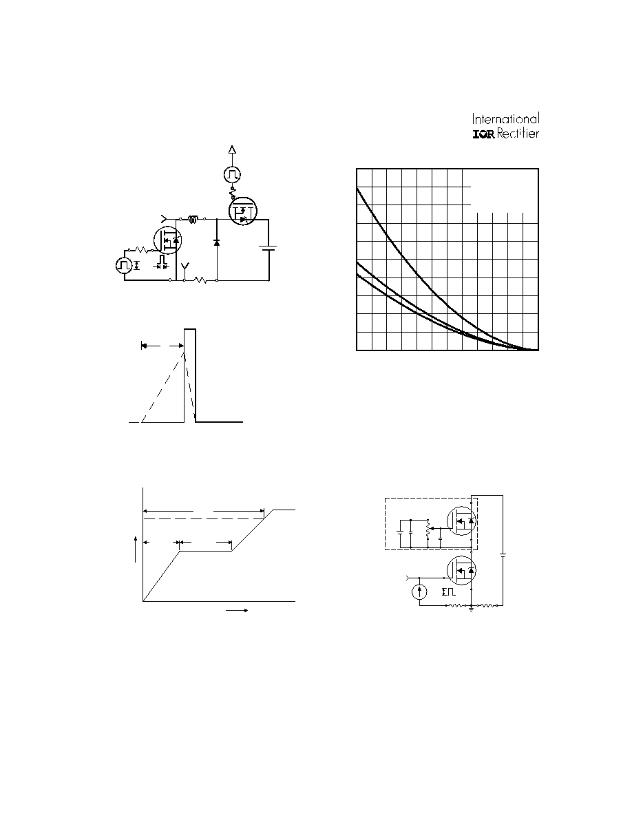
Fig 10a. Switching Time Test Circuit
V
DS
90%
10%
V
GS
t
d(on)
t
r
t
d(off)
t
f
Fig 10b. Switching Time Waveforms
V
DS
Pulse Width
1
µs
Duty Factor
0.1 %
R
D
V
GS
R
G
D.U.T.
10V
+
-
V
DD
Fig 11. Maximum Effective Transient Thermal Impedance, Junction-to-Case
Fig 9. Maximum Drain Current Vs.
Case Temperature
0.01
0.1
1
0.00001
0.0001
0.001
0.01
0.1
1
Notes:
1. Duty factor D =
t / t
2. Peak T = P
x Z
+ T
1
2
J
DM
thJC
C
P
t
t
DM
1
2
t , Rectangular Pulse Duration (sec)
Thermal Response
(Z )
1
thJC
0.01
0.02
0.05
0.10
0.20
D = 0.50
SINGLE PULSE
(THERMAL RESPONSE)
25
50
75
100
125
150
175
0
5
10
15
20
25
30
T , Case Temperature
( C)
I , Drain Current (A)
∞
C
D
IRFB/IRFS/IRFSL31N20D
6
www.irf.com
Q
G
Q
GS
Q
GD
V
G
Charge
D.U.T.
VDS
ID
IG
3mA
VGS
.3
µ
F
50K
.2
µ
F
12V
Current Regulator
Same Type as D.U.T.
Current Sampling Resistors
+
-
10 V
Fig 13b. Gate Charge Test Circuit
Fig 13a. Basic Gate Charge Waveform
Fig 12c. Maximum Avalanche Energy
Vs. Drain Current
Fig 12b. Unclamped Inductive Waveforms
Fig 12a. Unclamped Inductive Test Circuit
tp
V
(B R )D SS
I
A S
R G
I
A S
0 .0 1
tp
D .U .T
L
V D S
+
-
VD D
D R IV E R
A
1 5 V
2 0 V
25
50
75
100
125
150
175
0
200
400
600
800
1000
Starting T , Junction Temperature ( C)
E , Single Pulse Avalanche Energy (mJ)
J
AS
∞
ID
TOP
BOTTOM
7.3A
15A
18A
IRFB/IRFS/IRFSL31N20D
www.irf.com
7
P.W.
Period
di/dt
Diode Recovery
dv/dt
Ripple
5%
Body Diode
Forward Drop
Re-Applied
Voltage
Reverse
Recovery
Current
Body Diode Forward
Current
V
GS
=10V
V
DD
I
SD
Driver Gate Drive
D.U.T. I
SD
Waveform
D.U.T. V
DS
Waveform
Inductor Curent
D =
P.W.
Period
+
-
+
+
+
-
-
-
Fig 14. For N-channel HEXFET
Æ
Power MOSFETs
*
V
GS
= 5V for Logic Level Devices
Peak Diode Recovery dv/dt Test Circuit
R
G
V
DD
∑
dv/dt controlled by R
G
∑
Driver same type as D.U.T.
∑
I
SD
controlled by Duty Factor "D"
∑
D.U.T. - Device Under Test
D.U.T
Circuit Layout Considerations
∑
Low Stray Inductance
∑
Ground Plane
∑
Low Leakage Inductance
Current Transformer
*

IRFB/IRFS/IRFSL31N20D
8
www.irf.com
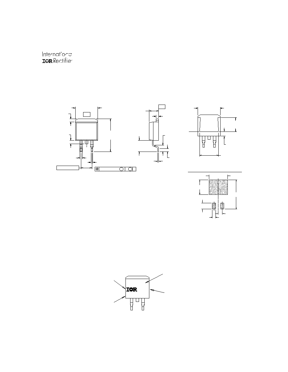
L E A D A S S IG N M E N T S
1 - G A T E
2 - D R A IN
3 - S O U R C E
4 - D R A IN
- B -
1 .3 2 (.0 5 2 )
1 .2 2 (.0 4 8 )
3 X
0 .5 5 (.0 2 2 )
0 .4 6 (.0 1 8 )
2 .9 2 ( .1 1 5 )
2 .6 4 ( .1 0 4 )
4 .6 9 ( .1 8 5 )
4 .2 0 ( .1 6 5 )
3 X
0 .9 3 ( .0 3 7 )
0 .6 9 ( .0 2 7 )
4 .0 6 ( .1 6 0 )
3 .5 5 ( .1 4 0 )
1 .1 5 (.0 4 5 )
M IN
6.4 7 (.2 5 5 )
6.1 0 (.2 4 0 )
3 .7 8 ( .1 4 9 )
3 .5 4 ( .1 3 9 )
- A -
1 0 .5 4 ( .4 1 5 )
1 0 .2 9 ( .4 0 5 )
2 .8 7 ( .1 1 3 )
2 .6 2 ( .1 0 3 )
1 5 .2 4 (.6 0 0 )
1 4 .8 4 (.5 8 4 )
1 4 .0 9 ( .5 5 5 )
1 3 .4 7 ( .5 3 0 )
3 X
1 .4 0 ( .0 5 5 )
1 .1 5 ( .0 4 5 )
2 .5 4 (.1 0 0)
2 X
0 .3 6 ( .0 1 4 ) M B A M
4
1 2 3
N O T E S :
1 D IM E N S IO N IN G & T O L E R A N C IN G P E R A N S I Y 1 4 .5 M , 1 9 8 2 . 3 O U T L IN E C O N F O R M S T O J E D E C O U T L IN E T O -2 2 0 A B .
2 C O N T R O L L IN G D IM E N S IO N : IN C H 4 H E A T S IN K & L E A D M E A S U R E M E N T S D O N O T IN C L U D E B U R R S .
TO-220AB Part Marking Information
TO-220AB Package Outline
Dimensions are shown in millimeters (inches)
P A R T N U M B E R
IN T E R N A T IO N A L
R E C T IF IE R
L O G O
E X A M P L E : T H IS IS A N IR F 1 0 1 0
W IT H A S S E M B L Y
L O T C O D E 9 B 1 M
A S S E M B L Y
L O T C O D E
D A T E C O D E
(Y Y W W )
Y Y = Y E A R
W W = W E E K
9 2 4 6
IR F 1 0 1 0
9 B 1 M
A
IRFB/IRFS/IRFSL31N20D
www.irf.com
9
D
2
Pak Package Outline
D
2
Pak Part Marking Information
1 0.16 (.4 00 )
RE F .
6.47 (.2 55 )
6.18 (.2 43 )
2.61 (.1 03 )
2.32 (.0 91 )
8.8 9 (.3 50 )
R E F .
- B -
1.3 2 (.05 2)
1.2 2 (.04 8)
2.7 9 (.110 )
2.2 9 (.090 )
1.3 9 (.0 5 5)
1.1 4 (.0 4 5)
5 .28 (.20 8)
4 .78 (.18 8)
4.69 (.1 85)
4.20 (.1 65)
1 0.54 (.4 15)
1 0.29 (.4 05)
- A -
2
1 3
15 .4 9 (.6 10)
14 .7 3 (.5 80)
3 X
0 .93 (.03 7 )
0 .69 (.02 7 )
5 .08 (.20 0)
3X
1.40 (.0 55)
1.14 (.0 45)
1.7 8 (.07 0)
1.2 7 (.05 0)
1.4 0 (.055 )
M AX.
NO TE S:
1 D IM EN S IO N S A F T ER SO L D ER D IP.
2 D IM EN S IO N IN G & T O LE RA N C IN G PE R A N S I Y1 4.5M , 198 2.
3 C O N T RO L LIN G D IM EN SIO N : IN C H .
4 H E AT SINK & L EA D D IM EN S IO N S D O N O T IN C LU D E B UR R S.
0.5 5 (.022 )
0.4 6 (.018 )
0 .25 (.01 0 ) M B A M
M IN IM U M R E CO M M E ND E D F O O TP R IN T
1 1.43 (.4 50 )
8.89 (.3 50 )
17 .78 (.70 0)
3 .8 1 (.15 0)
2 .08 (.08 2)
2X
LE A D A SS IG N M E N TS
1 - G A TE
2 - D R AIN
3 - S O U RC E
2.5 4 (.100 )
2 X
P A R T N U M B E R
IN TE R N A TIO N A L
R E C T IF IE R
L O G O
D A T E C O D E
(Y YW W )
YY = Y E A R
W W = W E E K
A S S E M B L Y
L O T C O D E
F 5 3 0 S
9 B 1 M
9 24 6
A

IRFB/IRFS/IRFSL31N20D
10
www.irf.com
TO-262 Part Marking Information
TO-262 Package Outline

IRFB/IRFS/IRFSL31N20D
www.irf.com
11
Repetitive rating; pulse width limited by
max. junction temperature.
I
SD
18A, di/dt
110A/µs, V
DD
V
(BR)DSS
,
T
J
175∞C
Notes:
Starting T
J
= 25∞C, L = 3.8mH
R
G
= 25
, I
AS
= 18A.
Pulse width
300µs; duty cycle
2%.
C
oss
eff. is a fixed capacitance that gives the same charging time
as C
oss
while V
DS
is rising from 0 to 80% V
DSS
WORLD HEADQUARTERS: 233 Kansas St., El Segundo, California 90245, Tel: (310) 252-7105
IR GREAT BRITAIN: Hurst Green, Oxted, Surrey RH8 9BB, UK Tel: ++ 44 1883 732020
IR CANADA: 15 Lincoln Court, Brampton, Ontario L6T3Z2, Tel: (905) 453 2200
IR GERMANY: Saalburgstrasse 157, 61350 Bad Homburg Tel: ++ 49 6172 96590
IR ITALY: Via Liguria 49, 10071 Borgaro, Torino Tel: ++ 39 11 451 0111
IR JAPAN: K&H Bldg., 2F, 30-4 Nishi-Ikebukuro 3-Chome, Toshima-Ku, Tokyo Japan 171 Tel: 81 3 3983 0086
IR SOUTHEAST ASIA: 1 Kim Seng Promenade, Great World City West Tower, 13-11, Singapore 237994 Tel: ++ 65 838 4630
IR TAIWAN:16 Fl. Suite D. 207, Sec. 2, Tun Haw South Road, Taipei, 10673, Taiwan Tel: 886-2-2377-9936
Data and specifications subject to change without notice. 2/2000
D
2
Pak Tape & Reel Information
3
4
4
TR R
FE E D D IR E C T IO N
1 .8 5 (.0 7 3 )
1 .6 5 (.0 6 5 )
1 .6 0 (.0 6 3 )
1 .5 0 (.0 5 9 )
4 .1 0 (.1 6 1 )
3 .9 0 (.1 5 3 )
T R L
F E E D D IR E C TIO N
10 .9 0 (.42 9 )
10 .7 0 (.42 1 )
1 6 .1 0 ( .6 3 4)
1 5 .9 0 ( .6 2 6)
1.7 5 (.0 69 )
1.2 5 (.0 49 )
1 1 .60 (.4 5 7 )
1 1 .40 (.4 4 9 )
15 .4 2 (.60 9 )
15 .2 2 (.60 1 )
4 .7 2 (.1 3 6)
4 .5 2 (.1 7 8)
2 4 .3 0 (.9 5 7 )
2 3 .9 0 (.9 4 1 )
0 .3 6 8 (.0 14 5 )
0 .3 4 2 (.0 13 5 )
1 .60 (.06 3 )
1 .50 (.05 9 )
1 3.50 (.5 32)
1 2.80 (.5 04)
3 30 .00
(1 4.1 73)
M A X.
2 7.40 (1.07 9)
2 3.90 (.941 )
6 0.00 (2.36 2)
M IN .
30 .4 0 (1.19 7)
M A X.
26 .40 (1.03 9)
24 .40 (.9 61 )
N O TE S :
1 . CO M FO R M S TO E IA- 418 .
2 . CO N TR O L LIN G D IM EN S IO N : M ILL IM ET E R .
3 . DIM EN S IO N M EA S UR E D @ H UB .
4 . IN C LU D ES F LA N G E D IS T O R T IO N @ O U T ER ED G E.
This is only applied to TO-220AB package
This is applied to D
2
Pak, when mounted on 1" square PCB ( FR-4 or G-10 Material ).
For recommended footprint and soldering techniques refer to application note #AN-994.