 | ÐлекÑÑоннÑй компоненÑ: IRFY9240 | СкаÑаÑÑ:  PDF PDF  ZIP ZIP |
Äîêóìåíòàöèÿ è îïèñàíèÿ www.docs.chipfind.ru
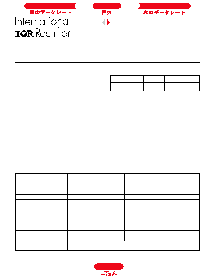
Product Summary
Part Number
BV
DSS
R
DS(on)
I
D
IRFY9240CM
-200V
0.51
-9.4A
Provisional Data Sheet No. PD 9.1295A
HEXFET
®
POWER MOSFET
International Rectifier's HEXFET technology is the key to
its advanced line of power MOSFET transistors. The effi-
cient geometry design achieves very low on-state resis-
tance combined with high transconductance.
HEXFET power MOSFETs also feature all of the well-
established advantages of MOSFETs, such as voltage
control, very fast switching, ease of paralleling and electri-
cal parameter temperature stability. They are well-suited
for applications such as switching power supplies, motor
controls, inverters, choppers, audio amplifiers, high en-
ergy pulse circuits, and virtually any application where
high reliability is required.
The HEXFET power MOSFET's totally isolated package
eliminates the need for additional isolating material between
the device and the heatsink. This improves ther mal effi-
ciency and reduces drain capacitance.
IRFY9240CM
Features
n
Hermetically Sealed
n
Electrically Isolated
n
Simple Drive Requirements
n
Ease of Paralleling
P-CHANNEL
-200 Volt, 0.51
HEXFET
Absolute Maximum Ratings
Parameter
IRFY9240CM
Units
ID @ VGS= -10V, TC = 25°C
Continuous Drain Current
-9.4
ID @ VGS= -10V, TC = 100°C
Continuous Drain Current
-6.0
A
IDM
Pulsed Drain Current
-36
PD @ TC = 25°C
Max. Power Dissipation
100
W
Linear Derating Factor
0.8
W/K
VGS
Gate-to-Source Voltage
±20
V
EAS
Single Pulse Avalance Energy
700
m J
IAR
Avalance Current
-9.4
A
EAR
Repetitive Avalanche Energy
10
m J
dv/dt
Peak Diode Recovery dv/dt
-5.5
V/ns
T J
Operating Junction
-55 to 150
Tstg
Storage Temperature Range
°C
Lead Temperature
300 (0.063 in (1.6mm) from case for 10 sec)
Weight
4.3(typical)
g
* I
D
current limited by pin diameter
Next Data Sheet
Index
Previous Datasheet
To Order
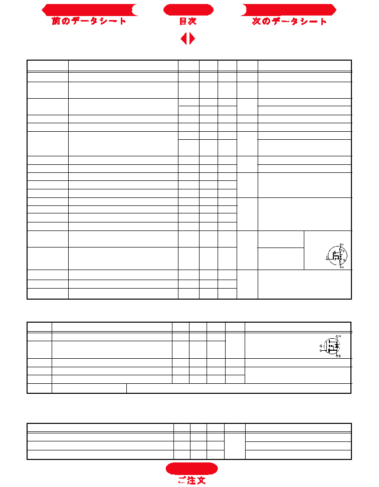
Electrical Characteristics
@ Tj = 25°C (Unless Otherwise Specified)
Parameter
Min
Typ
Max Units
Test Conditions
BVDSS
Drain-to-Source Breakdown Voltage
-200
--
--
V
VGS = 0V, ID = -1.0mA
BVDSS/
TJ Temperature Coefficient of Breakdown
--
-0.20
--
V/°C
Reference to 25°C, ID = -1.0mA
Voltage
RDS(on)
Static Drain-to-Source
--
--
0.51
VGS = -10V, ID = -6.0A
On-State Resistance
--
--
0.52
VGS = -10V, ID = -9.4A
VGS(th)
Gate Threshold Voltage
-2.0
--
-4.0
V
VDS = VGS, ID = -250
µ
A
gfs
Forward Transconductance
4.0
--
--
S (
) VDS
-15V, IDS = -6.0A
IDSS
Zero Gate Voltage Drain Current
--
--
-25
VDS
= 0.8 x max. rating,VGS = 0V
--
--
-250
VDS = 0.8 x max. rating
VGS = 0V, TJ = 125°C
IGSS
Gate-to-Source Leakage Forward
--
--
-100
VGS = -20V
IGSS
Gate-to-Source Leakage Reverse
--
--
100
VGS = 20V
Q g
Total Gate Charge
28
--
60
VGS = -10V, ID = -9.4A
Qgs
Gate-to-Source Charge
3.0
--
15
VDS = Max. Rating x 0.5
Qgd
Gate-to-Drain (`Miller') Charge
4.5
--
38
see figures 6 and 13
td(on)
Turn-On Delay Time
--
--
35
VDD = -100V, ID = -9.4A
tr
Rise Time
--
--
85
RG = 9.1
,
VGS = -10V
td(off)
Turn-Off Delay Time
--
--
85
tf
Fall Time
--
--
65
see figure 10
LD
Internal Drain Inductance
--
8.7
--
LS
Internal Source Inductance
--
8.7
--
Ciss
Input Capacitance
--
1200
--
VGS = 0v, VDS = -25V
Coss
Output Capacitance
--
570
--
pF
f = 1.0MHz.
Crss
Reverse Transfer Capacitance
--
81
--
see figure 5
Thermal Resistance
Parameter
Min Typ
Max Units
Test Conditions
RthJC Junction-to-Case
--
--
1.25
RthJA Junction-to-Ambient
--
--
80
K/W
Typical socket mount
RthCS Case-to-Sink
--
0.21
--
Mounting surface flat, smooth
µA
nC
nH
ns
Measured from the drain
lead, 6mm (0.25 in.) from
package to center of die.
Measured from the
source lead, 6mm (0.25
in.) from package to
source bonding pad.
Modified MOSFET symbol
showing the internal
inductances.
nA
Source-Drain Diode Ratings and Characteristics
Parameter
Min Typ Max Units
Test Conditions
IS
Continuous Source Current (Body Diode)
--
--
-9.4
ISM
Pulse Source Current (Body Diode)
--
--
-36
VSD
Diode Forward Voltage
--
--
-4.6
V
T
j
= 25°C, IS = -9.4A, VGS = 0V
trr
Reverse Recovery Time
--
--
440
ns
Tj = 25°C, IF = -9.4A, di/dt
-100 A/µs
QRR
Reverse Recovery Charge
--
--
7.2
µC
VDD
-50 V
ton
Forward Turn-On Time
Intrinsic turn-on time is negligible. Turn-on speed is substantially controlled by LS + LD.
IRFY9240CM Device
Modified MOSFET symbol showing the
integral reverse p-n junction rectifier.
A
Next Data Sheet
Index
Previous Datasheet
To Order
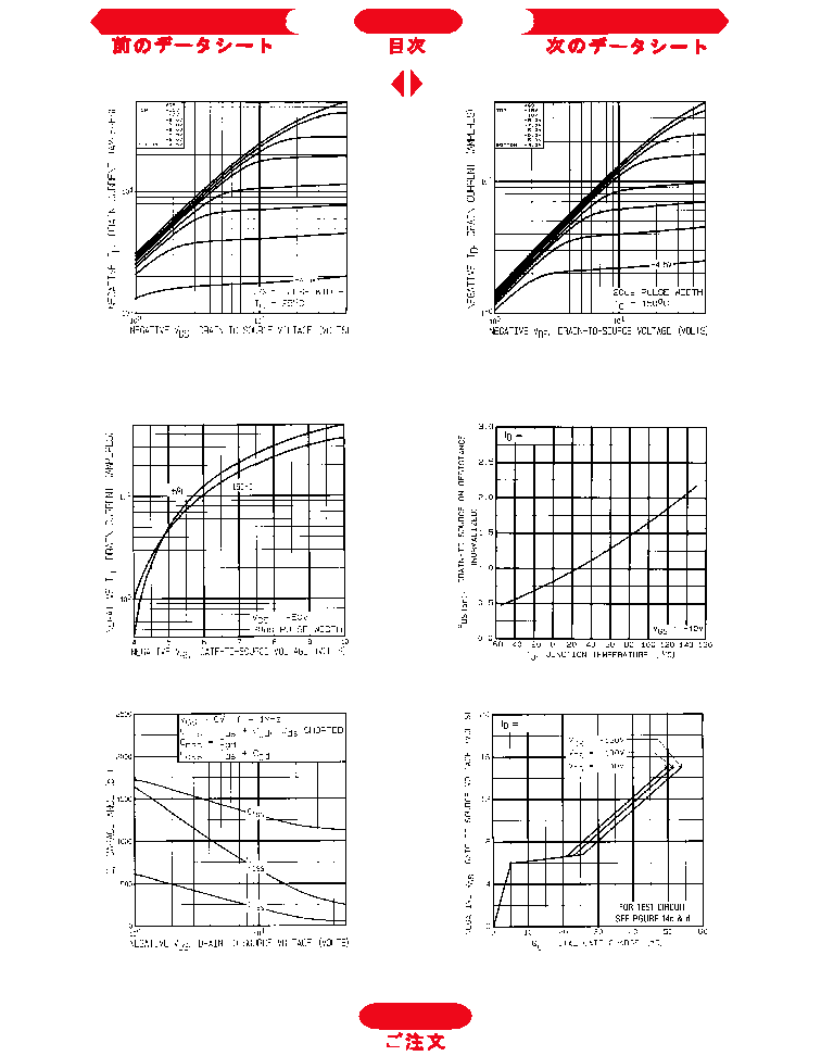
Fig. 5 -- Typical Capacitance vs. Drain-to-Source
Voltage
Fig. 6 -- Typical Gate Charge vs. Gate-to-Source
Voltage
Fig. 3 -- Typical Transfer Characteristics
Fig. 4 -- Normalized On-Resistance vs. Temperature
Fig. 1 -- Typical Output Characteristics
T
C
= 25°C
IRFY9240CM Device
Fig. 2 -- Typical Output Characteristics
T
C
= 150°C
-9.4
-9.4
To Order
Next Data Sheet
Index
Previous Datasheet
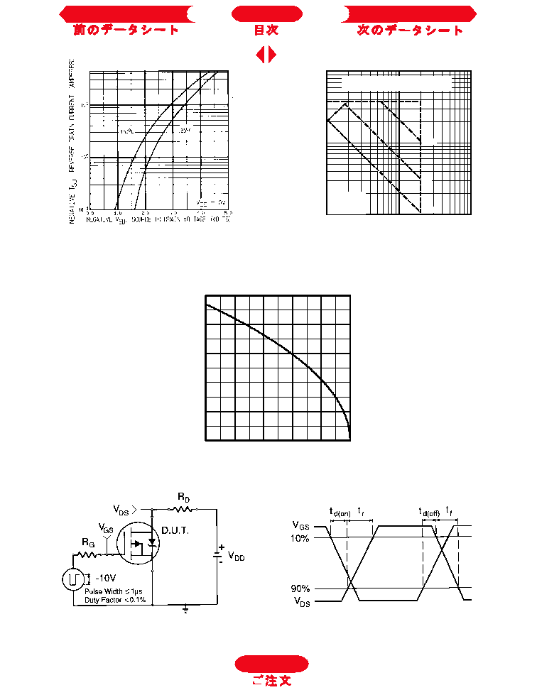
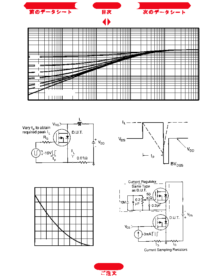
Fig. 10a -- Switching Time Test Circuit
Fig. 10b -- Switching Time Waveforms
Fig. 9 -- Maximum Drain Current vs. Case Tempera-
ture
Fig. 7 -- Typical Source-to-Drain Diode Forward
Voltage
Fig. 8 -- Maximum Safe Operating Area
IRFY9240CM Device
1
1 0
1 0 0
1 0
1 0 0
1 0 0 0
O P E R AT IO N I N T H IS A R E A L IM I T E D
B Y R
D S (o n )
T = 2 5 ° C
T = 1 5 0 °C
S ing le P uls e
C
J
1 0 ms
A
-I
,
D
r
a
i
n
C
u
rr
e
n
t
(A
)
-V , D ra in -to -S o u rc e V o lta g e ( V )
D S
D
10 0 µ s
1 m s
0
2
4
6
8
1 0
2 5
5 0
7 5
1 0 0
1 2 5
1 5 0
C
T , C as e Te m p er a tu r e ( °C )
A
Negativ
e I
D
, Drain Current (Amps)
To Order
Next Data Sheet
Index
Previous Datasheet
0 . 0 1
0 . 1
1
1 0
0 . 0 0 0 0 1
0 . 0 0 0 1
0 . 0 0 1
0 . 0 1
0 . 1
1
t , R e ctang ula r P u ls e D u ratio n (sec )
1
th
J
C
D = 0 . 50
0 .0 1
0 .0 2
0 .0 5
0 .1 0
0 .2 0
S I N G L E P U L S E
( T H E R M A L R E S P O N S E )
A
T
h
e
r
m
a
l
R
e
s
pons
e
(
Z
)
Fig. 11 -- Maximum Effective Transient Thermal Impedance, Junction-to-Case Vs. Pulse Duration
Fig. 12c -- Max. Avalanche Energy vs. Current
Fig. 12a -- Unclamped Inductive Test Circuit
Fig. 12b -- Unclamped Inductive Waveforms
Fig. 13a -- Gate Charge Test Circuit
IRFY9240CM Device
0
2 0 0
4 0 0
6 0 0
8 0 0
2 5
5 0
7 5
1 0 0
1 2 5
1 5 0
J
E
,
S
i
ngl
e
P
u
l
s
e A
v
al
an
c
h
e
E
n
er
g
y
(
m
J
)
AS
A
S ta rtin g T , J un c tion Te m p e ra tur e ( °C )
V = -50 V
I = -1 1A
To Order
Next Data Sheet
Index
Previous Datasheet