 | ÐлекÑÑоннÑй компоненÑ: IRFZ46NS | СкаÑаÑÑ:  PDF PDF  ZIP ZIP |
Äîêóìåíòàöèÿ è îïèñàíèÿ www.docs.chipfind.ru
IRFZ46NS
IRFZ46NL
HEXFET
®
Power MOSFET
l
Advanced Process Technology
l
Surface Mount (IRFZ46NS)
l
Low-profile through-hole (IRFZ46NL)
l
175°C Operating Temperature
l
Fast Switching
l
Fully Avalanche Rated
Parameter
Typ.
Max.
Units
R
JC
Junction-to-Case
1.4
R
JA
Junction-to-Ambient ( PCB Mounted,steady-state)**
40
Thermal Resistance
°C/W
Parameter
Max.
Units
I
D
@ T
C
= 25°C
Continuous Drain Current, V
GS
@ 10V
53
I
D
@ T
C
= 100°C
Continuous Drain Current, V
GS
@ 10V
37
A
I
DM
Pulsed Drain Current
180
P
D
@T
A
= 25°C
Power Dissipation
3.8
W
P
D
@T
C
= 25°C
Power Dissipation
107
W
Linear Derating Factor
0.71
W/°C
V
GS
Gate-to-Source Voltage
± 20
V
I
AR
Avalanche Current
28
A
E
AR
Repetitive Avalanche Energy
11
mJ
dv/dt
Peak Diode Recovery dv/dt
5.0
V/ns
T
J
Operating Junction and
-55 to + 175
T
STG
Storage Temperature Range
Soldering Temperature, for 10 seconds
300 (1.6mm from case )
°C
Absolute Maximum Ratings
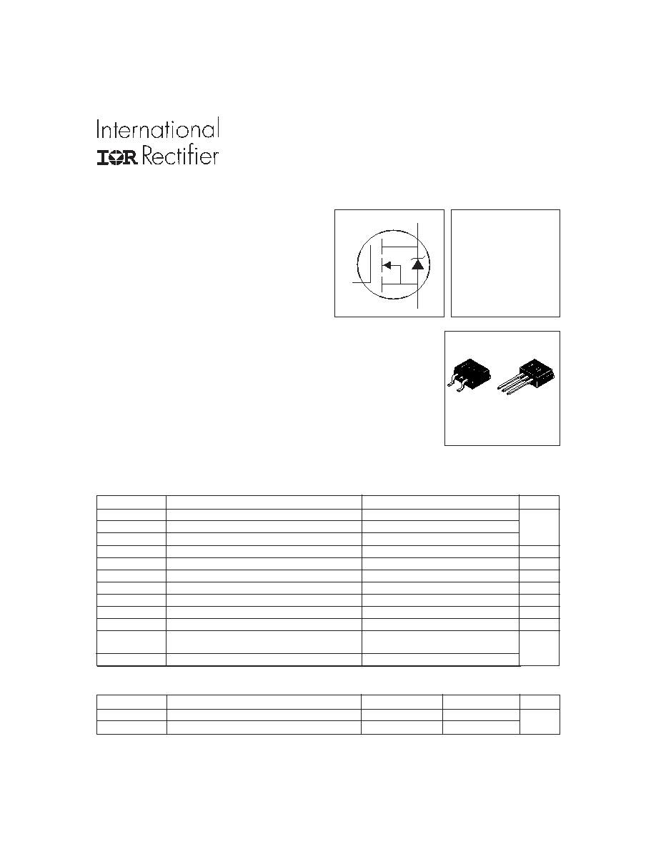
Advanced HEXFET
®
Power MOSFETs from International
Rectifier utilize advanced processing techniques to achieve
extremely low on-resistance per silicon area. This benefit,
combined with the fast switching speed and ruggedized
device design that HEXFET power MOSFETs are well known
for, provides the designer with an extremely efficient and
reliable device for use in a wide variety of applications.
The D
2
Pak is a surface mount power package capable of
accommodating die sizes up to HEX-4. It provides the highest
power capability and the lowest possible on-resistance in
any existing surface mount package. The D
2
Pak is suitable
for high current applications because of its low internal
connection resistance and can dissipate up to 2.0W in a
typical surface mount application.
The through-hole version (IRFZ46NL) is available for low-
profile applications.
Description
V
DSS
= 55V
R
DS(on)
= 0.0165
I
D
= 53A
2
D Pak
TO-262
S
D
G
04/08/04
www.irf.com
1
PD - 91305C
IRFZ46NS/IRFZ46NL
2
www.irf.com
Starting T
J
= 25°C, L = 389µH
R
G
= 25, I
AS
= 28A. (See Figure 12)
Repetitive rating; pulse width limited by
max. junction temperature. ( See fig. 11 )
Notes:
** When mounted on 1" square PCB (FR-4 or G-10 Material ).
For recommended footprint and soldering techniques refer to application note #AN-994.
I
SD
28A, di/dt 220A/µs, V
DD
V
(BR)DSS
,
T
J
175°C.
Pulse width 400µs; duty cycle 2%.
Uses IRFZ46N data and test conditions.
This is a typical value at device destruction and represents
operation outside rated limits.
This is a calculated value limited to TJ = 175
°C.
Calculated continuous current based on maximum allowable
junction temperature. Package limitation current is 39A.
Parameter
Min. Typ. Max. Units
Conditions
I
S
Continuous Source Current
MOSFET symbol
(Body Diode)
showing the
I
SM
Pulsed Source Current
integral reverse
(Body Diode)
p-n junction diode.
V
SD
Diode Forward Voltage
1.3
V
T
J
= 25°C, I
S
= 28A, V
GS
= 0V
t
rr
Reverse Recovery Time
67
101
ns
T
J
= 25°C, I
F
= 28A
Q
rr
Reverse Recovery Charge
208 312
nC
di/dt = 100A/µs
t
on
Forward Turn-On Time
Intrinsic turn-on time is negligible (turn-on is dominated by L
S
+L
D
)
Source-Drain Ratings and Characteristics
A
Parameter
Min. Typ. Max. Units
Conditions
V
(BR)DSS
Drain-to-Source Breakdown Voltage
55
V
V
GS
= 0V, I
D
= 250µA
V
(BR)DSS
/T
J
Breakdown Voltage Temp. Coefficient 0.057
V/°C Reference to 25°C, I
D
=1mA
R
DS(on)
Static Drain-to-Source On-Resistance
.0165
V
GS
=10V, I
D
= 28A
V
GS(th)
Gate Threshold Voltage
2.0
4.0
V
V
DS
= V
GS
, I
D
= 250µA
g
fs
Forward Transconductance
19
S
V
DS
= 25V, I
D
= 28A
25
µA
V
DS
= 55V, V
GS
= 0V
250
V
DS
= 44V, V
GS
= 0V, T
J
= 150°C
Gate-to-Source Forward Leakage
100
V
GS
= 20V
Gate-to-Source Reverse Leakage
-100
nA
V
GS
= -20V
Q
g
Total Gate Charge
72
I
D
= 28A
Q
gs
Gate-to-Source Charge
11
nC
V
DS
= 44V
Q
gd
Gate-to-Drain ("Miller") Charge
26
V
GS
= 10V, See Fig. 6 and 13
t
d(on)
Turn-On Delay Time
14
V
DD
= 28V
t
r
Rise Time
76
I
D
= 28A
t
d(off)
Turn-Off Delay Time
52
R
G
= 12
t
f
Fall Time
57
R
D
= 0.98, See Fig. 10
Between lead,
and center of die contact
C
iss
Input Capacitance
1696
V
GS
= 0V
C
oss
Output Capacitance
407
pF
V
DS
= 25V
C
rss
Reverse Transfer Capacitance
110
= 1.0MHz, See Fig. 5
E
AS
Single Pulse Avalanche Energy
583
152
I
AS
= 28A, L = 389mH
Electrical Characteristics @ T
J
= 25°C (unless otherwise specified)
I
GSS
ns
I
DSS
Drain-to-Source Leakage Current
nH
7.5
L
S
Internal Source Inductance
53
180
S
D
G
IRFZ46NS/IRFZ46NL
www.irf.com
3
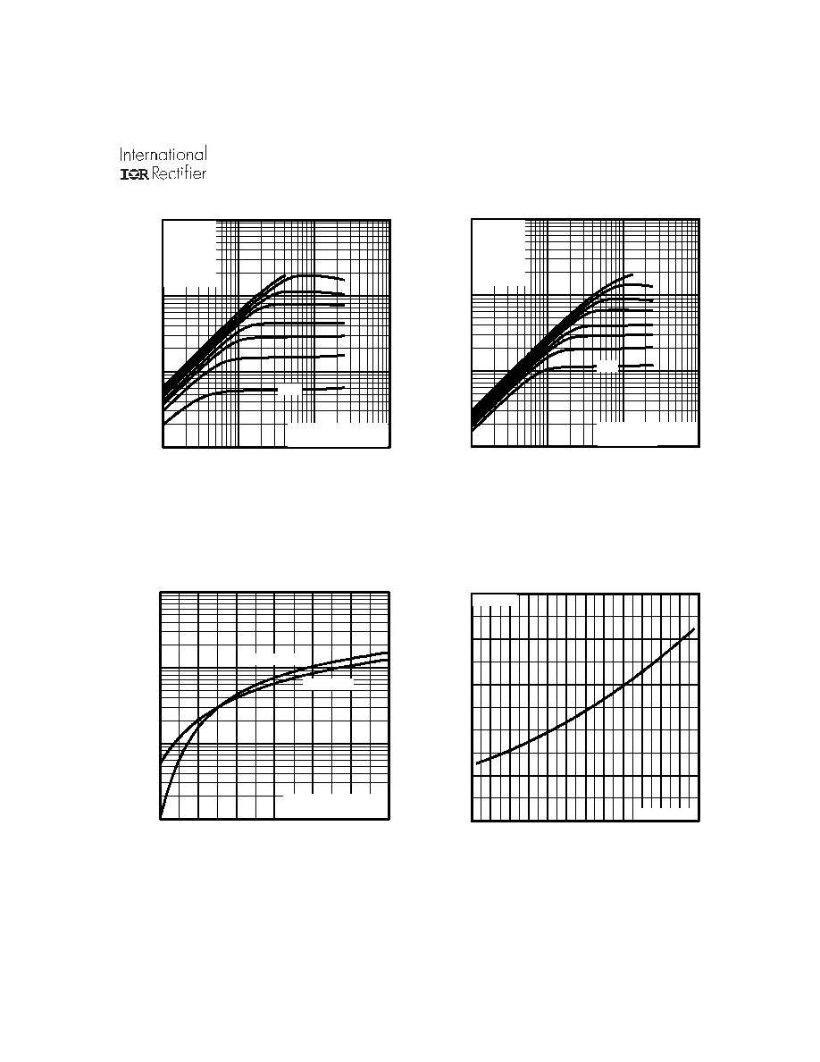
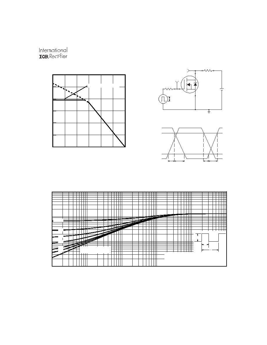
Fig 1. Typical Output Characteristics
Fig 3. Typical Transfer Characteristics
1
10
100
1000
0.1
1
10
100
I
,
D
r
ai
n-
t
o
-
S
ou
r
c
e C
u
r
r
e
nt
(
A
)
D
V , Drain-to-Source Voltage (V)
DS
VGS
TOP 15V
10V
8.0V
7.0V
6.0V
5.5V
5.0V
BOTTOM 4.5V
20µs PULSE WIDTH
T = 25°C
C
A
4.5V
1
10
100
1000
0.1
1
10
100
4.5V
I , D
r
a
i
n
-
to
-S
o
u
rc
e
C
u
rre
n
t
(A
)
D
V , Drain-to-Source Voltage (V)
DS
VGS
TOP 15V
10V
8.0V
7.0V
6.0V
5.5V
5.0V
BOTTOM 4.5V
20µs PULSE WIDTH
T = 175°C
C
A
0.0
0.5
1.0
1.5
2.0
2.5
-60 -40 -20
0
20
40
60
80
100 120 140 160 180
J
T , Junction Temperature (°C)
R
, D
r
a
i
n
-
to
-
S
o
u
rc
e
O
n
R
e
s
i
s
t
a
n
c
e
DS
(
on)
(N
o
r
m
a
l
i
ze
d)
V = 10V
GS
A
I = 46A
D
1
10
100
1000
4
5
6
7
8
9
10
T = 25°C
J
GS
V , Gate-to-Source Voltage (V)
D
I
, Dra
i
n
-
to
-
S
o
u
rc
e
C
u
rre
n
t
(A)
T = 175°C
J
A
V = 25V
20µs PULSE WIDTH
DS
Fig 4. Normalized On-Resistance
Vs. Temperature
Fig 2. Typical Output Characteristics
T
J
= 25°C
T
J
= 175°C
IRFZ46NS/IRFZ46NL
4
www.irf.com
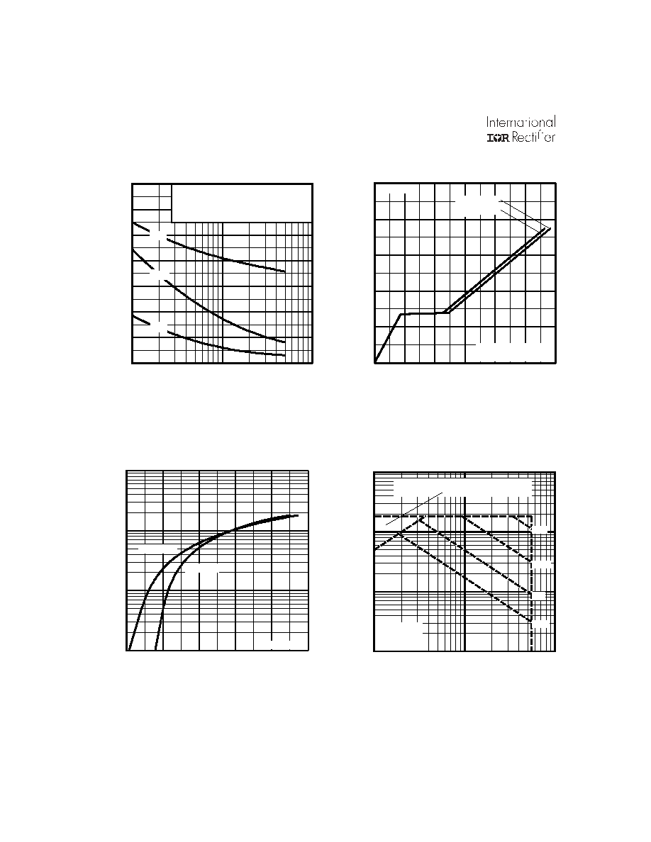
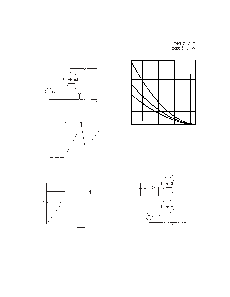
Fig 7. Typical Source-Drain Diode
Forward Voltage
Fig 5. Typical Capacitance Vs.
Drain-to-Source Voltage
Fig 8. Maximum Safe Operating Area
Fig 6. Typical Gate Charge Vs.
Gate-to-Source Voltage
0
4
8
12
16
20
0
10
20
30
40
50
60
Q , Total Gate Charge (nC)
G
V
, G
a
te
-to
-
S
o
u
r
c
e
V
o
l
t
a
g
e
(V
)
GS
A
FOR TEST CIRCUIT
SEE FIGURE 13
V = 44V
V = 28V
I = 28A
D
DS
DS
1
10
100
1000
0.4
0.8
1.2
1.6
2.0
2.4
T = 25°C
J
V = 0V
GS
V , Source-to-Drain Voltage (V)
I , R
e
v
e
rs
e
D
r
a
i
n
C
u
rre
n
t
(A
)
SD
SD
A
T = 175°C
J
1
10
100
1000
1
10
100
V , Drain-to-Source Voltage (V)
DS
I , D
r
a
i
n
C
u
rre
n
t
(A
)
OPERATION IN THIS AREA LIMITED
BY R
D
DS(on)
10µs
100µs
1ms
10ms
A
T = 25°C
T = 175°C
Single Pulse
C
J
0
400
800
1200
1600
2000
2400
2800
1
10
100
C
,
C
a
p
a
c
i
ta
n
c
e
(p
F
)
DS
V , Drain-to-Source Voltage (V)
A
V = 0V, f = 1MHz
C = C + C , C SHORTED
C = C
C = C + C
GS
iss gs gd ds
rss gd
oss ds gd
C
iss
C
oss
C
rss
IRFZ46NS/IRFZ46NL
www.irf.com
5
Fig 9. Maximum Drain Current Vs.
Case Temperature
Fig 10a. Switching Time Test Circuit
V
DS
90%
10%
V
GS
t
d(on)
t
r
t
d(off)
t
f
Fig 10b. Switching Time Waveforms
Fig 11. Maximum Effective Transient Thermal Impedance, Junction-to-Case
V
DS
Pulse Width 1 µs
Duty Factor 0.1 %
R
D
V
GS
R
G
D.U.T.
10V
+
-
V
DD
0.01
0.1
1
10
0.00001
0.0001
0.001
0.01
0.1
1
Notes:
1. Duty factor D =
t / t
2. Peak T = P
x Z
+ T
1
2
J
DM
thJC
C
P
t
t
DM
1
2
t , Rectangular Pulse Duration (sec)
Ther
m
a
l
R
e
sponse
(Z
)
1
thJC
0.01
0.02
0.05
0.10
0.20
D = 0.50
SINGLE PULSE
(THERMAL RESPONSE)
25
50
75
100
125
150
175
TC , Case Temperature (°C)
0
10
20
30
40
50
60
I D
,
D
r
a
i
n
C
u
r
r
e
n
t
(
A
)
Limited By Package
IRFZ46NS/IRFZ46NL
6
www.irf.com
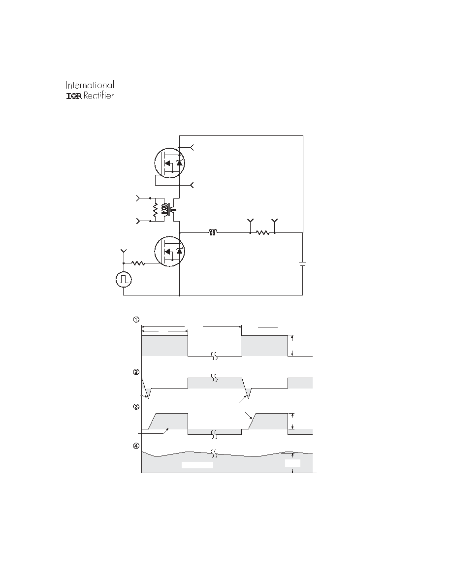
Fig 12a. Unclamped Inductive Test Circuit
Fig 12b. Unclamped Inductive Waveforms
Fig 13a. Basic Gate Charge Waveform
V
DS
L
D.U.T.
V
DD
I
AS
t
p
0.01
R
G
+
-
t
p
V
DS
I
AS
V
DD
V
(BR)DSS
10 V
D.U.T.
V
DS
I
D
I
G
3mA
V
GS
.3
µ
F
50K
.2
µ
F
12V
Current Regulator
Same Type as D.U.T.
Current Sampling Resistors
+
-
Fig 13b. Gate Charge Test Circuit
Q
G
Q
GS
Q
GD
V
G
Charge
10 V
Fig 12c. Maximum Avalanche Energy
Vs. Drain Current
0
100
200
300
400
500
25
50
75
100
125
150
175
J
E
, S
i
n
g
le
P
u
ls
e
A
v
a
l
a
n
c
h
e
E
n
e
r
g
y
(
m
J
)
AS
A
Starting T , Junction Temperature (°C)
V = 25V
I
TOP 11A
20A
BOTTOM 28A
DD
D
IRFZ46NS/IRFZ46NL
www.irf.com
7
Peak Diode Recovery dv/dt Test Circuit
P.W.
Period
di/dt
Diode Recovery
dv/dt
Ripple
5%
Body Diode
Forward Drop
Re-Applied
Voltage
Reverse
Recovery
Current
Body Diode Forward
Current
V
GS
=10V
V
DD
I
SD
Driver Gate Drive
D.U.T. I
SD
Waveform
D.U.T. V
DS
Waveform
Inductor Curent
D =
P.W.
Period
+
-
+
+
+
-
-
-
Fig 14. For N-Channel HEXFETS
*
V
GS
= 5V for Logic Level Devices
R
G
V
DD
· dv/dt controlled by R
G
· Driver same type as D.U.T.
· I
SD
controlled by Duty Factor "D"
· D.U.T. - Device Under Test
D.U.T
Circuit Layout Considerations
· Low Stray Inductance
· Ground Plane
· Low Leakage Inductance
Current Transformer
*
IRFZ46NS/IRFZ46NL
8
www.irf.com
D
2
Pak Package Outline
D
2
Pak
Part Marking Information
10.16 (.400)
REF.
6.47 (.255)
6.18 (.243)
2.61 (.103)
2.32 (.091)
8.89 (.350)
REF.
- B -
1.32 (.052)
1.22 (.048)
2.79 (.110)
2.29 (.090)
1.39 (.055)
1.14 (.045)
5.28 (.208)
4.78 (.188)
4.69 (.185)
4.20 (.165)
10.54 (.415)
10.29 (.405)
- A -
2
1 3
15.49 (.610)
14.73 (.580)
3X
0.93 (.037)
0.69 (.027)
5.08 (.200)
3X
1.40 (.055)
1.14 (.045)
1.78 (.070)
1.27 (.050)
1.40 (.055)
MAX.
NOTES:
1 DIMENSIONS AFTER SOLDER DIP.
2 DIMENSIONING & TOLERANCING PER ANSI Y14.5M, 1982.
3 CONTROLLING DIMENSION : INCH.
4 HEATSINK & LEAD DIMENSIONS DO NOT INCLUDE BURRS.
0.55 (.022)
0.46 (.018)
0.25 (.010) M B A M
MINIMUM RECOMMENDED FOOTPRINT
11.43 (.450)
8.89 (.350)
17.78 (.700)
3.81 (.150)
2.08 (.082)
2X
LEAD ASSIGNMENTS
1 - GATE
2 - DRAIN
3 - SOURCE
2.54 (.100)
2X
PART NUMBER
INTERNATIONAL
RECTIFIER
LOGO
DATE CODE
(YYWW)
YY = YEAR
WW = WEEK
ASSEMBLY
LOT CODE
F530S
9B 1M
9246
A
IRFZ46NS/IRFZ46NL
www.irf.com
9
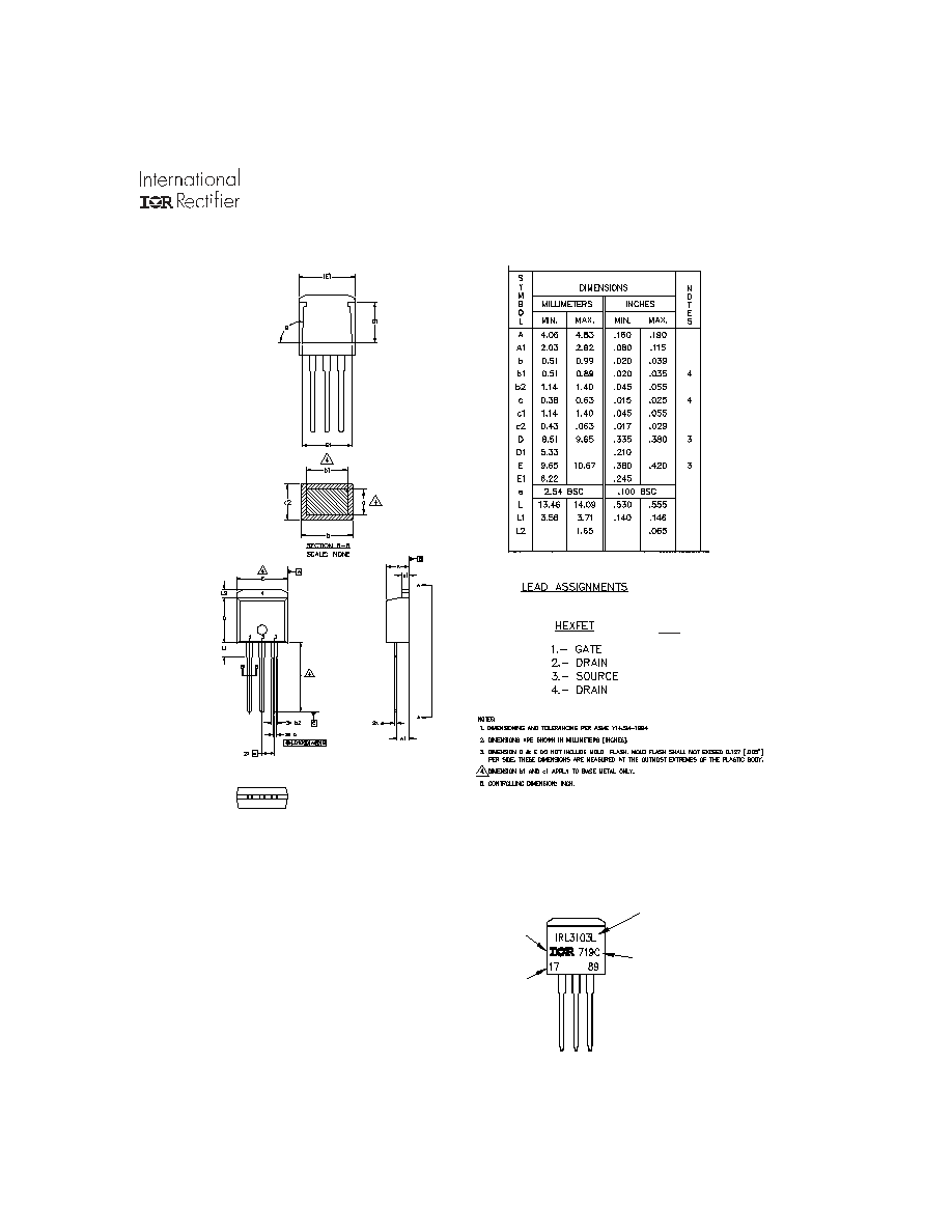
TO-262 Package Outline
Dimensions are shown in millimeters (inches)
TO-262 Part Marking Information
@ Y 6 H Q G @ ) U C D T Ã D T Ã 6 I Ã D S G " " G
G P U Ã 8 P 9 @ Ã & ' (
6 T T @ H 7 G `
Q 6 S U Ã I V H 7 @ S
9 6 U @ Ã 8 P 9 @
X @ @ F Ã (
G D I @ Ã 8
G P U Ã 8 P 9 @
` @ 6 S Ã & Ã 2 Ã ( ( &
6 T T @ H 7 G @ 9 Ã P I Ã X X Ã ( Ã ( ( &
D I Ã U C @ Ã 6 T T @ H 7 G ` Ã G D I @ Ã Å 8 Å
G P B P
S @ 8 U D A D @ S
D I U @ S I 6 U D P I 6 G
IGBT
1- GATE
2- COLLECTOR
3- EMITTER
IRFZ46NS/IRFZ46NL
10
www.irf.com
Data and specifications subject to change without notice.
This product has been designed and qualified for the industrial market.
Qualification Standards can be found on IR's Web site.
IR WORLD HEADQUARTERS: 233 Kansas St., El Segundo, California 90245, USA Tel: (310) 252-7105
TAC Fax: (310) 252-7903
Visit us at www.irf.com for sales contact information. 4/04
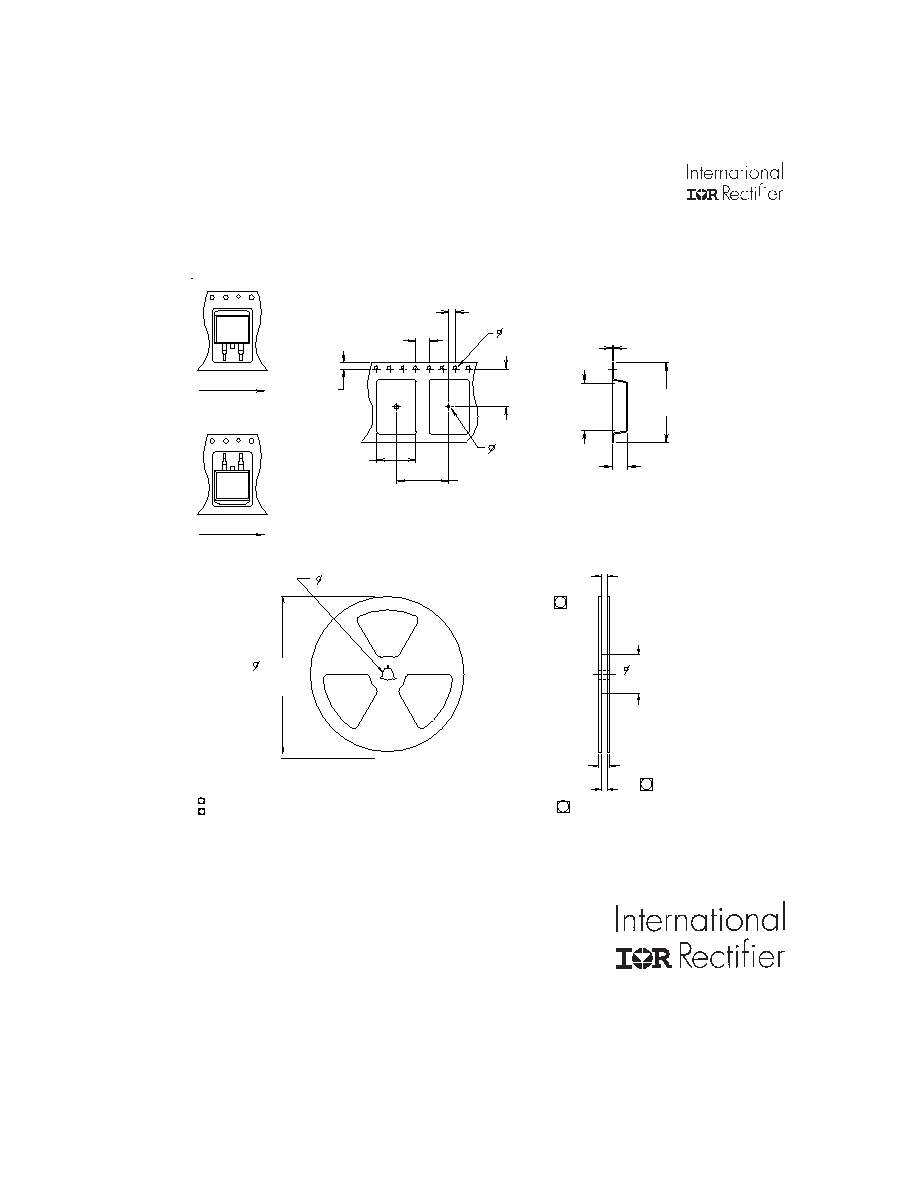
Tape & Reel Information
D
2
Pak
3
4
4
TRR
FEED DIRECTION
1.85 (.073)
1.65 (.065)
1.60 (.063)
1.50 (.059)
4.10 (.161)
3.90 (.153)
TRL
FEED DIRECTION
10.90 (.429)
10.70 (.421)
16.10 (.634)
15.90 (.626)
1.75 (.069)
1.25 (.049)
11.60 (.457)
11.40 (.449)
15.42 (.609)
15.22 (.601)
4.72 (.136)
4.52 (.178)
24.30 (.957)
23.90 (.941)
0.368 (.0145)
0.342 (.0135)
1.60 (.063)
1.50 (.059)
13.50 (.532)
12.80 (.504)
330.00
(14.173)
MAX.
27.40 (1.079)
23.90 (.941)
60.00 (2.362)
MIN.
30.40 (1.197)
MAX.
26.40 (1.039)
24.40 (.961)
NOTES :
1. COMFORMS TO EIA-418.
2. CONTROLLING DIMENSION: MILLIMETER.
3. DIMENSION MEASURED @ HUB.
4. INCLUDES FLANGE DISTORTION @ OUTER EDGE.