Äîêóìåíòàöèÿ è îïèñàíèÿ www.docs.chipfind.ru
IRG4BC15MD
INSULATED GATE BIPOLAR TRANSISTOR WITH
ULTRAFAST SOFT RECOVERY DIODE
Features
Features
Features
Features
Features
E
G
n-ch an nel
C
V
CES
= 600V
V
CE(on) typ.
= 1.88V
@V
GE
= 15V, I
C
= 8.6A
Parameter
Min.
Typ.
Max.
Units
R
JC
Junction-to-Case - IGBT
2.7
R
JC
Junction-to-Case - Diode
7.0
°C/W
R
CS
Case-to-Sink, flat, greased surface
0.50
R
JA
Junction-to-Ambient, typical socket mount
80
Wt
Weight
2 (0.07)
g (oz)
Thermal Resistance
5/25/01
Absolute Maximum Ratings
Parameter
Max.
Units
V
CES
Collector-to-Emitter Voltage
600
V
I
C
@ T
C
= 25°C
Continuous Collector Current
14
I
C
@ T
C
= 100°C
Continuous Collector Current
8.6
I
CM
Pulsed Collector Current
28
A
I
LM
Clamped Inductive Load Current
28
I
F
@ T
C
= 100°C
Diode Continuous Forward Current
4.0
t
sc
Short Circuit Withstand Time
12
µs
I
FM
Diode Maximum Forward Current
16
A
V
GE
Gate-to-Emitter Voltage
± 20
V
P
D
@ T
C
= 25°C
Maximum Power Dissipation
49
P
D
@ T
C
= 100°C
Maximum Power Dissipation
19
T
J
Operating Junction and
-55 to +150
T
STG
Storage Temperature Range
°C
Soldering Temperature, for 10 sec.
300 (0.063 in. (1.6mm) from case)
Mounting Torque, 6-32 or M3 Screw.
10 lbf·in (1.1 N·m)
·
Rugged: 10µsec short circuit capable at VGS = 15V
·
Low VCE(on) for 4 to 10kHz applications
·
IGBT co-packaged with ultra-soft-recovery anti-parallel
diodes
·
Industry standard TO-220AB package
Benefits
·
Best Value for Appliance and Industrial applications
·
Offers highest efficiency and short circuit capability for
intermediate applications
·
Provides best efficiency for the mid range frequency
(4 to 10kHz)
·
Optimized for Appliance and Industrial applications up to
1HP
·
High noise immune "Positive Only" gate drive - Negative
bias gate drive not necessary
·
For Low EMI designs - requires little or no snubbing
·
Single Package switch for bridge circuit applications
·
Compatible with high voltage Gate Drive IC's
·
Allows simpler gate drive
PD- 94151A
W
TO-220AB
www.irf.com
1
Short Circuit Rated
Fast IGBT
IRG4BC15MD
Parameter
Min. Typ. Max. Units
Conditions
Q
g
Total Gate Charge (turn-on)
46
I
C
= 8.6A
Qge
Gate - Emitter Charge (turn-on)
4.2
nC
V
CC
= 400V
Q
gc
Gate - Collector Charge (turn-on)
15
V
GE
= 15V
t
d(on)
Turn-On Delay Time
21
T
J
= 25°C
t
r
Rise Time
38
ns
I
C
= 8.6A, V
CC
= 480V
t
d(off)
Turn-Off Delay Time
540
810
V
GE
= 15V, R
G
= 75
t
f
Fall Time
350
530
Energy losses include "tail" and
E
on
Turn-On Switching Loss
0.32
diode reverse recovery.
E
off
Turn-Off Switching Loss
1.93
mJ
E
ts
Total Switching Loss
2.25
3.6
t
d(on)
Turn-On Delay Time
20
T
J
= 150°C,
t
r
Rise Time
42
ns
I
C
= 8.6A, V
CC
= 480V
t
d(off)
Turn-Off Delay Time
650
V
GE
= 15V, R
G
= 75
t
f
Fall Time
590
Energy losses include "tail" and
E
ts
Total Switching Loss
3.0
mJ
diode reverse recovery.
L
E
Internal Emitter Inductance
7.5
nH
Measured 5mm from package
C
ies
Input Capacitance
340
V
GE
= 0V
C
oes
Output Capacitance
35
pF
V
CC
= 30V
C
res
Reverse Transfer Capacitance
8.8
= 1.0MHz
t
rr
Diode Reverse Recovery Time
28
42
ns
T
J
= 25°C
38
57
T
J
= 125°C
I
F
= 4.0A
I
rr
Diode Peak Reverse Recovery Current
2.9
5.2
A
T
J
= 25°C
3.7
6.7
T
J
= 125°C V
R
= 200V
Q
rr
Diode Reverse Recovery Charge
40
60
nC
T
J
= 25°C
70
110
T
J
= 125°C di/dt 200A/µs
di
(rec)M
/dt
Diode Peak Rate of Fall of Recovery
280
A/µs
T
J
= 25°C
During t
b
240
T
J
= 125°C
Parameter
Min. Typ. Max. Units
Conditions
V
(BR)CES
Collector-to-Emitter Breakdown Voltage
600
V
V
GE
= 0V, I
C
= 250µA
V
(BR)CES
/
T
J
Temperature Coeff. of Breakdown Voltage
0.65
V/°C
V
GE
= 0V, I
C
= 1.0mA
V
CE(on)
Collector-to-Emitter Saturation Voltage
1.88
2.3
I
C
= 8.6A
V
GE
= 15V
2.6
V
I
C
= 14A
2.1
I
C
= 8.6A, T
J
= 150°C
V
GE(th)
Gate Threshold Voltage
4.0
6.5
V
CE
= V
GE
, I
C
= 250µA
V
GE(th)
/
T
J
Temperature Coeff. of Threshold Voltage
-10
mV/°C V
CE
= V
GE
, I
C
= 250µA
g
fe
Forward Transconductance
2.3
3.4
S
V
CE
= 100V, I
C
= 6.5A
I
CES
Zero Gate Voltage Collector Current
250
µA
V
GE
= 0V, V
CE
= 600V
1400
V
GE
= 0V, V
CE
= 600V, T
J
= 150°C
V
FM
Diode Forward Voltage Drop
1.5
1.8
V
I
C
= 4.0A
1.4
1.7
I
C
= 4.0A, T
J
= 150°C
I
GES
Gate-to-Emitter Leakage Current
±100
nA
V
GE
= ±20V
Switching Characteristics @ T
J
= 25°C (unless otherwise specified)
Electrical Characteristics @ T
J
= 25°C (unless otherwise specified)
IRG4BC15MD
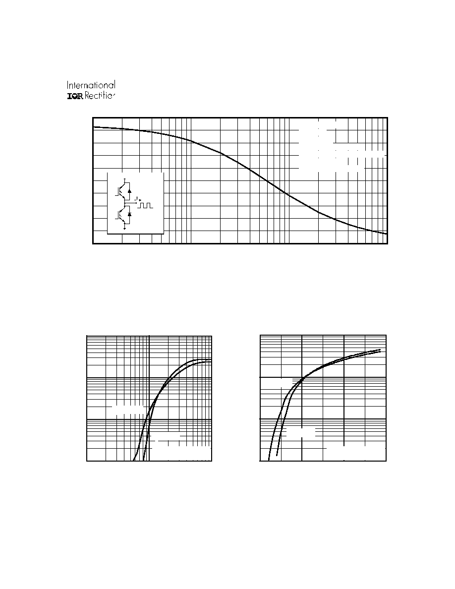
Fig. 1 - Typical Load Current vs. Frequency
(Load Current = I
RMS
of fundamental)
Fig. 2 - Typical Output Characteristics
Fig. 3 - Typical Transfer Characteristics
0.1
1
10
100
0.1
1
10
V , Collector-to-Emitter Voltage (V)
I , Collector-to-Emitter Current (A)
CE
C
V = 15V
20µs PULSE WIDTH
GE
T = 25 C
J
°
T = 150 C
J
°
0.1
1
10
100
5.0
10.0
15.0
20.0
V , Gate-to-Emitter Voltage (V)
I , Collector-to-Emitter Current (A)
GE
C
V = 50V
5µs PULSE WIDTH
CC
T = 150 C
J
°
T = 25 C
J
°
0.1
1
10
100
f , Frequency ( kHz )
0
2
4
6
8
10
Load Current ( A )
Duty cycle : 50%
Tj = 125°C
Tsink = 90°C
Gate drive as specified
Turn-on losses include effects of
reverse recovery
Power Dissipation = 11W
60% of rated
voltage
Ideal diodes
IRG4BC15MD
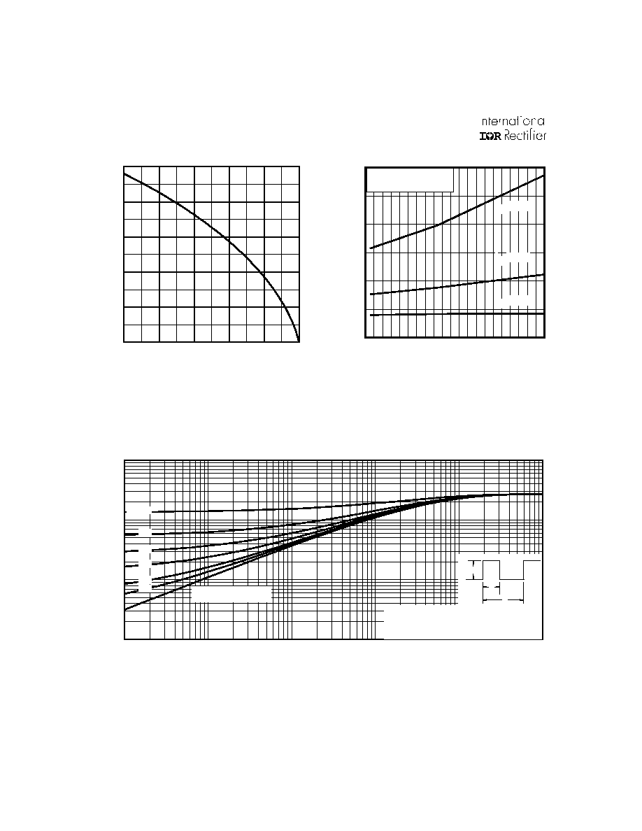
Fig. 6 - Maximum Effective Transient Thermal Impedance, Junction-to-Case
Fig. 5 - Typical Collector-to-Emitter Voltage
vs. Junction Temperature
Fig. 4 - Maximum Collector Current vs. Case
Temperature
0.01
0.1
1
10
0.00001
0.0001
0.001
0.01
0.1
1
Notes:
1. Duty factor D = t / t
2. Peak T = P
x Z
+ T
1
2
J
DM
thJC
C
P
t
t
DM
1
2
t , Rectangular Pulse Duration (sec)
Thermal Response (Z )
1
thJC
0.01
0.02
0.05
0.10
0.20
D = 0.50
SINGLE PULSE
(THERMAL RESPONSE)
25
50
75
100
125
150
0
3
6
9
12
15
T , Case Temperature ( C)
Maximum DC Collector Current(A)
C
°
-60 -40 -20
0
20
40
60
80
100 120 140
TJ , Junction Temperature (°C)
1.0
2.0
3.0
4.0
V
CE
, Collector-to Emitter Voltage (V)
IC = 17A
VGE = 15V
80µs PULSE WIDTH
IC = 9.0A
IC = 4.3A
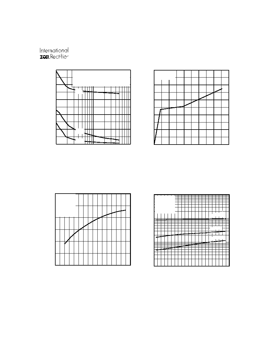
IRG4BC15MD
Fig. 7 - Typical Capacitance vs.
Collector-to-Emitter Voltage
Fig. 8 - Typical Gate Charge vs.
Gate-to-Emitter Voltage
Fig. 9 - Typical Switching Losses vs. Gate
Resistance
Fig. 10 - Typical Switching Losses vs.
Junction Temperature
0
10
20
30
40
50
0
4
8
12
16
20
Q , Total Gate Charge (nC)
V , Gate-to-Emitter Voltage (V)
G
GE
V
= 400V
I
= 9.0A
CC
C
0
10
20
30
40
50
60
70
80
RG, Gate Resistance (
)
2.00
2.10
2.20
2.30
Total Switching Losses (mJ)
VCC = 480V
VGE = 15V
TJ = 25°C
I C = 8.6A
-60 -40 -20
0
20
40
60
80 100 120 140 160
TJ, Junction Temperature (°C)
0.1
1
10
100
Total Switching Losses (mJ)
RG = 75
VGE = 15V
VCC = 480V
IC = 17A
IC = 9.0A
IC = 4.3A
1
10
100
0
100
200
300
400
500
V , Collector-to-Emitter Voltage (V)
C, Capacitance (pF)
CE
V
C
C
C
=
=
=
=
0V,
C
C
C
f = 1MHz
+ C
+ C
C SHORTED
GE
ies
ge
gc ,
ce
res
gc
oes
ce
gc
C
ies
C
oes
C
res