 | ÐлекÑÑоннÑй компоненÑ: IRG4BC30W | СкаÑаÑÑ:  PDF PDF  ZIP ZIP |
Äîêóìåíòàöèÿ è îïèñàíèÿ www.docs.chipfind.ru
Parameter
Max.
Units
V
CES
Collector-to-Emitter Breakdown Voltage
600
V
I
C
@ T
C
= 25°C
Continuous Collector Current
23
I
C
@ T
C
= 100°C
Continuous Collector Current
12
A
I
CM
Pulsed Collector Current
Q
92
I
LM
Clamped Inductive Load Current
R
92
V
GE
Gate-to-Emitter Voltage
± 20
V
E
ARV
Reverse Voltage Avalanche Energy
S
180
mJ
P
D
@ T
C
= 25°C
Maximum Power Dissipation
100
P
D
@ T
C
= 100°C
Maximum Power Dissipation
42
T
J
Operating Junction and
-55 to + 150
T
STG
Storage Temperature Range
Soldering Temperature, for 10 seconds
300 (0.063 in. (1.6mm from case )
°C
Mounting torque, 6-32 or M3 screw.
10 lbf·in (1.1N·m)
IRG4BC30W
INSULATED GATE BIPOLAR TRANSISTOR
PD - 91629A
E
C
G
n-channel
Features
Features
Features
Features
Features
· Designed expressly for Switch-Mode Power
Supply and PFC (power factor correction)
applications
· Industry-benchmark switching losses improve
efficiency of all power supply topologies
· 50% reduction of Eoff parameter
· Low IGBT conduction losses
· Latest-generation IGBT design and construction offers
tighter parameters distribution, exceptional reliability
· Lower switching losses allow more cost-effective
operation than power MOSFETs up to 150 kHz
("hard switched" mode)
· Of particular benefit to single-ended converters and
boost PFC topologies 150W and higher
· Low conduction losses and minimal minority-carrier
recombination make these an excellent option for
resonant mode switching as well (up to >>300 kHz)
Benefits
V
CES
= 600V
V
CE(on) max.
=
2.70V
@V
GE
= 15V, I
C
= 12A
4/24/2000
Parameter
Typ.
Max.
Units
R
JC
Junction-to-Case
1.2
R
CS
Case-to-Sink, Flat, Greased Surface
0.50
°C/W
R
JA
Junction-to-Ambient, typical socket mount
80
Wt
Weight
1.44
g
Thermal Resistance
Absolute Maximum Ratings
W
TO-220AB
www.irf.com
1
IRG4BC30W
2
www.irf.com
Parameter
Min. Typ. Max. Units
Conditions
Q
g
Total Gate Charge (turn-on)
--
51
76
I
C
= 12A
Q
ge
Gate - Emitter Charge (turn-on)
--
7.6
11
nC
V
CC
= 400V
See Fig.8
Q
gc
Gate - Collector Charge (turn-on)
--
18
27
V
GE
= 15V
t
d(on)
Turn-On Delay Time
--
25
--
t
r
Rise Time
--
16
--
T
J
= 25°C
t
d(off)
Turn-Off Delay Time
--
99
150
I
C
= 12A, V
CC
= 480V
t
f
Fall Time
--
67
100
V
GE
= 15V, R
G
= 23
E
on
Turn-On Switching Loss
--
0.13
--
Energy losses include "tail"
E
off
Turn-Off Switching Loss
--
0.13
--
mJ
See Fig. 9, 10, 13, 14
E
ts
Total Switching Loss
--
0.26 0.35
t
d(on)
Turn-On Delay Time
--
24
--
T
J
= 150°C,
t
r
Rise Time
--
17
--
I
C
= 12A, V
CC
= 480V
t
d(off)
Turn-Off Delay Time
--
150
--
V
GE
= 15V, R
G
= 23
t
f
Fall Time
--
150
--
Energy losses include "tail"
E
ts
Total Switching Loss
--
0.55
--
mJ
See Fig. 11,13, 14
L
E
Internal Emitter Inductance
--
7.5
--
nH
Measured 5mm from package
C
ies
Input Capacitance
--
980
--
V
GE
= 0V
C
oes
Output Capacitance
--
71
--
pF
V
CC
= 30V
See Fig. 7
C
res
Reverse Transfer Capacitance
--
18
--
= 1.0MHz
Parameter
Min. Typ. Max. Units
Conditions
V
(BR)CES
Collector-to-Emitter Breakdown Voltage
600
--
--
V
V
GE
= 0V, I
C
= 250µA
V
(BR)ECS
Emitter-to-Collector Breakdown Voltage
T
18
--
--
V
V
GE
= 0V, I
C
= 1.0A
V
(BR)CES
/
T
J
Temperature Coeff. of Breakdown Voltage
--
0.34
--
V/°C
V
GE
= 0V, I
C
= 1.0mA
--
2.1
2.7
I
C
= 12A V
GE
= 15V
V
CE(ON)
Collector-to-Emitter Saturation Voltage
--
2.45
--
I
C
= 23A
See Fig.2, 5
--
1.95
--
I
C
= 12A , T
J
= 150°C
V
GE(th)
Gate Threshold Voltage
3.0
--
6.0
V
CE
= V
GE
, I
C
= 250µA
V
GE(th)
/
T
J
Temperature Coeff. of Threshold Voltage
--
-11
--
mV/°C V
CE
= V
GE
, I
C
= 250µA
g
fe
Forward Transconductance
U
11
16
--
S
V
CE
=
100 V, I
C
= 12A
--
--
250
V
GE
= 0V, V
CE
= 600V
--
--
2.0
V
GE
= 0V, V
CE
= 10V, T
J
= 25°C
--
--
1000
V
GE
= 0V, V
CE
= 600V, T
J
= 150°C
I
GES
Gate-to-Emitter Leakage Current
--
--
±100
n A
V
GE
= ±20V
Electrical Characteristics @ T
J
= 25°C (unless otherwise specified)
I
CES
Zero Gate Voltage Collector Current
V
µ A
Switching Characteristics @ T
J
= 25°C (unless otherwise specified)
ns
ns
T
Pulse width
80µs; duty factor
0.1%.
U
Pulse width 5.0µs, single shot.
Notes:
Q
Repetitive rating; V
GE
= 20V, pulse width limited by
max. junction temperature. ( See fig. 13b )
R
V
CC
= 80%(V
CES
), V
GE
= 20V, L = 10µH, R
G
= 23
,
(See fig. 13a)
S
Repetitive rating; pulse width limited by maximum
junction temperature.
IRG4BC30W
www.irf.com
3
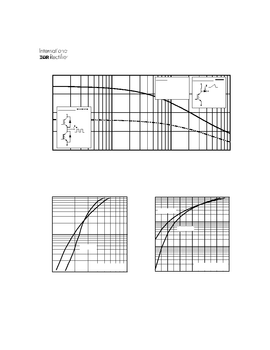
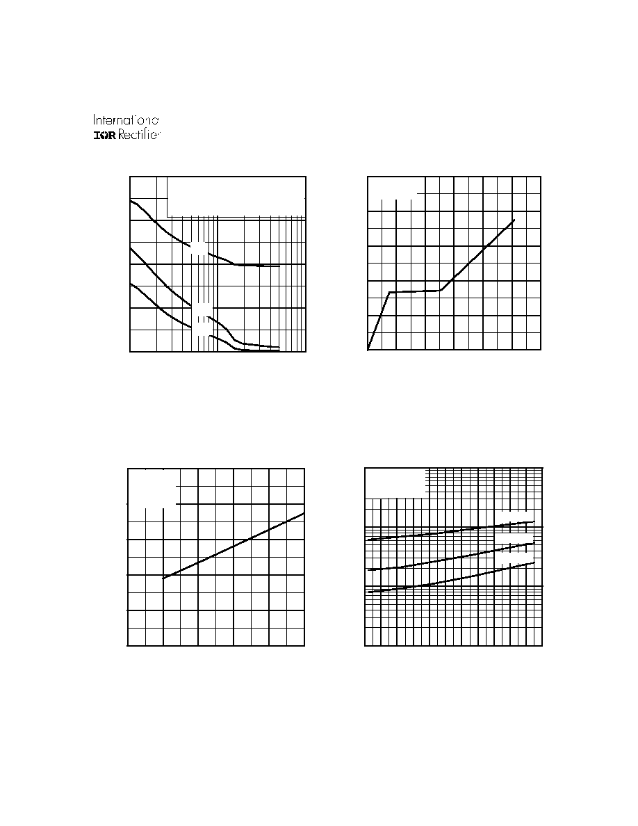
Fig. 1 - Typical Load Current vs. Frequency
(For square wave, I=I
RMS
of fundamental; for triangular wave, I=I
PK
)
Fig. 2 - Typical Output Characteristics
Fig. 3 - Typical Transfer Characteristics
Load Current ( A )
0
1 0
2 0
3 0
4 0
0 . 1
1
1 0
1 0 0
f, Frequenc y (k Hz)
A
6 0 % o f ra te d
vo l t a g e
Id e a l d io de s
S q u a re wa ve:
F o r b o t h :
D uty c y c le : 5 0%
T = 1 2 5° C
T = 90 °C
G a te d rive a s s pe c ified
s in k
J
T ri a n g u la r w a v e :
C la m p vo lt a g e :
8 0 % o f r a t e d
P o w e r D i s si p a tio n = 2 1 W
1
10
100
1
10
V , Collector-to-Emitter Voltage (V)
I , Collector-to-Emitter Current (A)
CE
C
V = 15V
20µs PULSE WIDTH
GE
T = 25 C
J
°
T = 150 C
J
°
0.1
1
10
100
5.0
6.0
7.0
8.0
9.0
10.0
11.0
V , Gate-to-Emitter Voltage (V)
I , Collector-to-Emitter Current (A)
GE
C
V = 50V
5µs PULSE WIDTH
CC
T = 25 C
J
°
T = 150 C
J
°
IRG4BC30W
4
www.irf.com
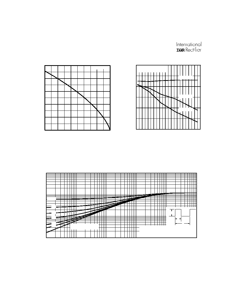
0.01
0.1
1
10
0.00001
0.0001
0.001
0.01
0.1
1
Notes:
1. Duty factor D = t / t
2. Peak T = P
x Z
+ T
1
2
J
DM
thJC
C
P
t
t
DM
1
2
t , Rectangular Pulse Duration (sec)
Thermal Response (Z )
1
thJC
0.01
0.02
0.05
0.10
0.20
D = 0.50
SINGLE PULSE
(THERMAL RESPONSE)
Fig. 6 - Maximum Effective Transient Thermal Impedance, Junction-to-Case
Fig. 5 - Collector-to-Emitter Voltage vs.
Junction Temperature
Fig. 4 - Maximum Collector Current vs. Case
Temperature
0
5
1 0
1 5
2 0
2 5
2 5
5 0
7 5
1 0 0
1 2 5
1 5 0
Ma
x
i
m
u
m
D
C
C
o
l
l
e
c
t
o
r
Cu
r
r
e
n
t
(
A
T , C a s e T e m p e ra tu re (°C )
C
V = 1 5 V
G E
A
-60 -40 -20
0
20
40
60
80 100 120 140 160
1.5
2.0
2.5
3.0
T , Junction Temperature ( C)
V , Collector-to-Emitter Voltage(V)
J
°
CE
V = 15V
80 us PULSE WIDTH
GE
I = A
24
C
I = A
12
C
I = A
6
C
IRG4BC30W
www.irf.com
5
0
10
20
30
40
50
0.0
0.1
0.2
0.3
0.4
0.5
R , Gate Resistance (Ohm)
Total Switching Losses (mJ)
G
V = 480V
V = 15V
T = 25 C
I = 12A
CC
GE
J
C
°
-60 -40 -20
0
20
40
60
80 100 120 140 160
0.01
0.1
1
10
T , Junction Temperature ( C )
Total Switching Losses (mJ)
J
°
R = Ohm
V = 15V
V = 480V
G
GE
CC
I = A
24
C
I = A
12
C
I = A
6
C
Fig. 10 - Typical Switching Losses vs.
Junction Temperature
Fig. 9 - Typical Switching Losses vs. Gate
Resistance
Fig. 8 - Typical Gate Charge vs.
Gate-to-Emitter Voltage
Fig. 7 - Typical Capacitance vs.
Collector-to-Emitter Voltage
1
10
100
0
500
1000
1500
2000
V , Collector-to-Emitter Voltage (V)
C, Capacitance (pF)
CE
V
C
C
C
=
=
=
=
0V,
C
C
C
f = 1MHz
+ C
+ C
C SHORTED
GE
ies
ge
gc ,
ce
res
gc
oes
ce
gc
Cies
Coes
Cres
23
R
G
, Gate Resistance
(
)
0
10
20
30
40
50
60
0
4
8
12
16
20
Q , Total Gate Charge (nC)
V , Gate-to-Emitter Voltage (V)
G
GE
V
= 400V
I
= 12A
CC
C