 | ÐлекÑÑоннÑй компоненÑ: IRG4BC40K | СкаÑаÑÑ:  PDF PDF  ZIP ZIP |
Äîêóìåíòàöèÿ è îïèñàíèÿ www.docs.chipfind.ru
4/17/2000
Parameter
Max.
Units
V
CES
Collector-to-Emitter Voltage
600
V
I
C
@ T
C
= 25°C
Continuous Collector Current
42
I
C
@ T
C
= 100°C
Continuous Collector Current
25
A
I
CM
Pulsed Collector Current
Q
84
I
LM
Clamped Inductive Load Current
R
84
t
sc
Short Circuit Withstand Time
10
µs
V
GE
Gate-to-Emitter Voltage
±20
V
E
ARV
Reverse Voltage Avalanche Energy
S
15
mJ
P
D
@ T
C
= 25°C
Maximum Power Dissipation
160
W
P
D
@ T
C
= 100°C
Maximum Power Dissipation
65
T
J
Operating Junction and
-55 to +150
T
STG
Storage Temperature Range
°C
Soldering Temperature, for 10 sec.
300 (0.063 in. (1.6mm) from case)
Mounting torque, 6-32 or M3 screw.
10 lbf·in (1.1N·m)
IRG4BC40K
Short Circuit Rated
UltraFast IGBT
INSULATED GATE BIPOLAR TRANSISTOR
PD - 91592B
Parameter
Typ.
Max.
Units
R
JC
Junction-to-Case
0.77
R
CS
Case-to-Sink, Flat, Greased Surface
0.50
°C/W
R
JA
Junction-to-Ambient, typical socket mount
80
Wt
Weight
2 (0.07)
g (oz)
Thermal Resistance
Absolute Maximum Ratings
TO-220AB
V
CES
= 600V
V
CE(on) typ.
= 2.1V
@V
GE
= 15V, I
C
= 25A
Features
Features
Features
Features
Features
· Short Circuit Rated UltraFast: optimized for high
operating frequencies >5.0 kHz , and Short Circuit
Rated to 10µs @ 125°C, V
GE
= 15V
· Generation 4 IGBT design provides higher efficiency
than Generation 3
· Industry standard TO-247AC package
· Generation 4 IGBTs offer highest efficiency available
· IGBTs optimized for specified application conditions
Benefits
E
C
G
n-channel
www.irf.com
1
IRG4BC40K
2
www.irf.com
Parameter
Min. Typ. Max. Units
Conditions
Q
g
Total Gate Charge (turn-on)
--
120
180
I
C
= 25A
Q
ge
Gate - Emitter Charge (turn-on)
--
16
24
nC
V
CC
= 400V
See Fig.8
Q
gc
Gate - Collector Charge (turn-on)
--
51
77
V
GE
= 15V
t
d(on)
Turn-On Delay Time
--
30
--
t
r
Rise Time
--
15
--
T
J
= 25°C
t
d(off)
Turn-Off Delay Time
--
140
210
I
C
= 25A, V
CC
= 480V
t
f
Fall Time
--
140
210
V
GE
= 15V, R
G
= 10
E
on
Turn-On Switching Loss
--
0.62
--
Energy losses include "tail"
E
off
Turn-Off Switching Loss
--
0.33
--
mJ
See Fig. 9,10,14
E
ts
Total Switching Loss
--
0.95
1.4
t
sc
Short Circuit Withstand Time
10
--
--
µs
V
CC
= 400V, T
J
= 125°C
V
GE
= 15V, R
G
= 10
, V
CPK
< 500V
t
d(on)
Turn-On Delay Time
--
30
--
T
J
= 150°C,
t
r
Rise Time
--
18
--
I
C
= 25A, V
CC
= 480V
t
d(off)
Turn-Off Delay Time
--
190
--
V
GE
= 15V, R
G
= 10
t
f
Fall Time
--
150
--
Energy losses include "tail"
E
ts
Total Switching Loss
--
1.9
--
mJ
See Fig. 11,14
L
E
Internal Emitter Inductance
--
13
--
nH
Measured 5mm from package
C
ies
Input Capacitance
--
1600
--
V
GE
= 0V
C
oes
Output Capacitance
--
130
--
pF
V
CC
= 30V
See Fig. 7
C
res
Reverse Transfer Capacitance
--
55
--
= 1.0MHz
Parameter
Min. Typ. Max. Units
Conditions
V
(BR)CES
Collector-to-Emitter Breakdown Voltage
600
--
--
V
V
GE
= 0V, I
C
= 250µA
V
(BR)ECS
Emitter-to-Collector Breakdown Voltage
T
18
--
--
V
V
GE
= 0V, I
C
= 1.0A
V
(BR)CES
/
T
J
Temperature Coeff. of Breakdown Voltage
--
0.46
--
V/°C
V
GE
= 0V, I
C
= 1.0mA
--
2.10
2.6
I
C
= 25A V
GE
= 15V
V
CE(ON)
Collector-to-Emitter Saturation Voltage
--
2.70
--
I
C
= 42A
See Fig.2, 5
--
2.14
--
I
C
= 25A , T
J
= 150°C
V
GE(th)
Gate Threshold Voltage
3.0
--
6.0
V
CE
= V
GE
, I
C
= 250µA
V
GE(th)
/
T
J
Temperature Coeff. of Threshold Voltage
--
-13
--
mV/°C V
CE
= V
GE
, I
C
= 250µA
g
fe
Forward Transconductance
U
7.0
14
--
S
V
CE
= 100 V, I
C
= 25A
--
--
250
V
GE
= 0V, V
CE
= 600V
--
--
2.0
V
GE
= 0V, V
CE
= 10V, T
J
= 25°C
--
--
2000
V
GE
= 0V, V
CE
= 600V, T
J
= 150°C
I
GES
Gate-to-Emitter Leakage Current
--
--
±100
n A
V
GE
= ±20V
Electrical Characteristics @ T
J
= 25°C (unless otherwise specified)
I
CES
Zero Gate Voltage Collector Current
V
µ A
Switching Characteristics @ T
J
= 25°C (unless otherwise specified)
ns
ns
S
Repetitive rating; pulse width limited by maximum
junction temperature.
T
Pulse width
80µs; duty factor 0.1%.
U
Pulse width 5.0µs, single shot.
Notes:
Q
Repetitive rating; V
GE
= 20V, pulse width limited by
max. junction temperature. ( See fig. 13b )
R
V
CC
= 80%(V
CES
), V
GE
= 20V, L = 10µH, R
G
= 10
,
(See fig. 13a)
IRG4BC40K
www.irf.com
3
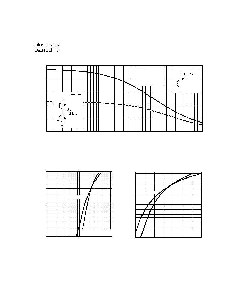
Fig. 1 - Typical Load Current vs. Frequency
(Load Current = I
RMS
of fundamental)
Fig. 2 - Typical Output Characteristics
Fig. 3 - Typical Transfer Characteristics
1
1 0
1 0 0
5
7
9
1 1
C
I , Collector-to-Emitter Current (A)
G E
T = 25°C
T = 150°C
J
J
V , Gate-to-Emitter Voltage (V)
A
V = 50V
5 µ s P U L S E W I D T H
C C
1
10
100
0.1
1
10
V , Collector-to-Emitter Voltage (V)
I , Collector-to-Emitter Current (A)
CE
C
V = 15V
20µs PULSE WIDTH
GE
T = 25 C
J
o
T = 150 C
J
o
0
1 0
2 0
3 0
4 0
5 0
0 . 1
1
1 0
1 0 0
f, Frequency (kHz)
Load Current (A)
A
6 0 % o f ra te d
v o lta g e
Ide a l d io de s
S q u a re w a v e :
F o r b o t h:
D u ty c y c le : 5 0 %
T = 1 2 5 ° C
T = 9 0 ° C
G a te d riv e a s s p e c ifie d
sink
J
T ria n g u la r w a v e :
C la m p v o lta g e :
8 0 % o f ra te d
P o w e r D is s ip a t io n = 2 8 W
IRG4BC40K
4
www.irf.com
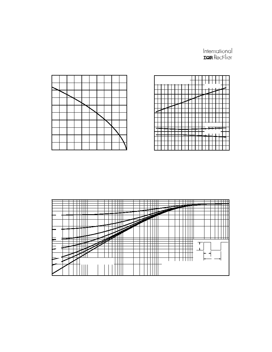
Fig. 6 - Maximum Effective Transient Thermal Impedance, Junction-to-Case
Fig. 5 - Typical Collector-to-Emitter Voltage
vs. Junction Temperature
Fig. 4 - Maximum Collector Current vs. Case
Temperature
-60 -40 -20
0
20
40
60
80 100 120 140 160
1.0
2.0
3.0
4.0
5.0
T , Junction Temperature ( C)
V , Collector-to-Emitter Voltage(V)
J
°
CE
V = 15V
80 us PULSE WIDTH
GE
I = A
12.5
C
I = A
25
C
I = A
50
C
25
50
75
100
125
150
0
10
20
30
40
50
T , Case Temperature ( C)
Maximum DC Collector Current(A)
C
°
0.01
0.1
1
0.00001
0.0001
0.001
0.01
0.1
1
Notes:
1. Duty factor D = t / t
2. Peak T = P
x Z
+ T
1
2
J
DM
thJC
C
P
t
t
DM
1
2
t , Rectangular Pulse Duration (sec)
Thermal Response (Z )
1
thJC
0.01
0.02
0.05
0.10
0.20
0.50
SINGLE PULSE
(THERMAL RESPONSE)
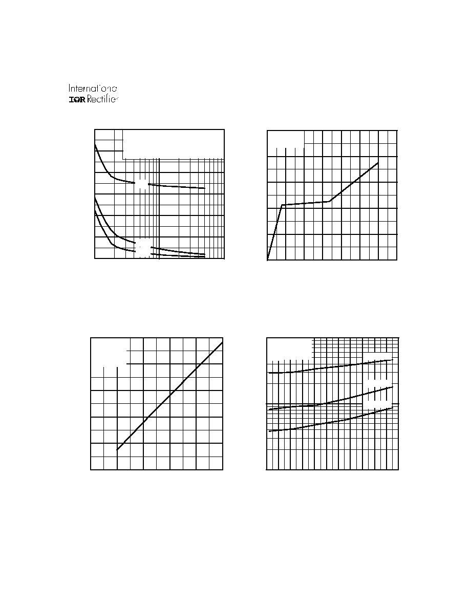
IRG4BC40K
www.irf.com
5
Fig. 7 - Typical Capacitance vs.
Collector-to-Emitter Voltage
Fig. 8 - Typical Gate Charge vs.
Gate-to-Emitter Voltage
0
20
40
60
80
100
120
140
0
4
8
12
16
20
Q , Total Gate Charge (nC)
V , Gate-to-Emitter Voltage (V)
G
GE
V
= 400V
I
= 25A
CC
C
1
10
100
0
500
1000
1500
2000
2500
3000
V , Collector-to-Emitter Voltage (V)
C, Capacitance (pF)
CE
V
C
C
C
=
=
=
=
0V,
C
C
C
f = 1MHz
+ C
+ C
C SHORTED
GE
ies
ge
gc ,
ce
res
gc
oes
ce
gc
Cies
Coes
Cres
Fig. 9 - Typical Switching Losses vs. Gate
Resistance
Fig. 10 - Typical Switching Losses vs.
Junction Temperature
0
10
20
30
40
50
0.80
1.00
1.20
1.40
1.60
1.80
R , Gate Resistance (Ohm)
Total Switching Losses (mJ)
G
V = 480V
V = 15V
T = 25 C
I = 25A
CC
GE
J
C
°
-60 -40 -20
0
20
40
60
80 100 120 140 160
0.1
1
10
T , Junction Temperature ( C )
Total Switching Losses (mJ)
J
°
R = 10Ohm
V = 15V
V = 480V
G
GE
CC
I = A
50
C
I = A
25
C
I = A
12.5
C