 | ÐлекÑÑоннÑй компоненÑ: IRG4PC40F | СкаÑаÑÑ:  PDF PDF  ZIP ZIP |
Äîêóìåíòàöèÿ è îïèñàíèÿ www.docs.chipfind.ru
Parameter
Max.
Units
V
CES
Collector-to-Emitter Breakdown Voltage
600
V
I
C
@ T
C
= 25°C
Continuous Collector Current
49
I
C
@ T
C
= 100°C
Continuous Collector Current
27
A
I
CM
Pulsed Collector Current
Q
200
I
LM
Clamped Inductive Load Current
R
200
V
GE
Gate-to-Emitter Voltage
± 20
V
E
ARV
Reverse Voltage Avalanche Energy
S
15
mJ
P
D
@ T
C
= 25°C
Maximum Power Dissipation
160
P
D
@ T
C
= 100°C
Maximum Power Dissipation
65
T
J
Operating Junction and
-55 to + 150
T
STG
Storage Temperature Range
Soldering Temperature, for 10 seconds
300 (0.063 in. (1.6mm from case )
°C
Mounting torque, 6-32 or M3 screw.
10 lbf·in (1.1N·m)
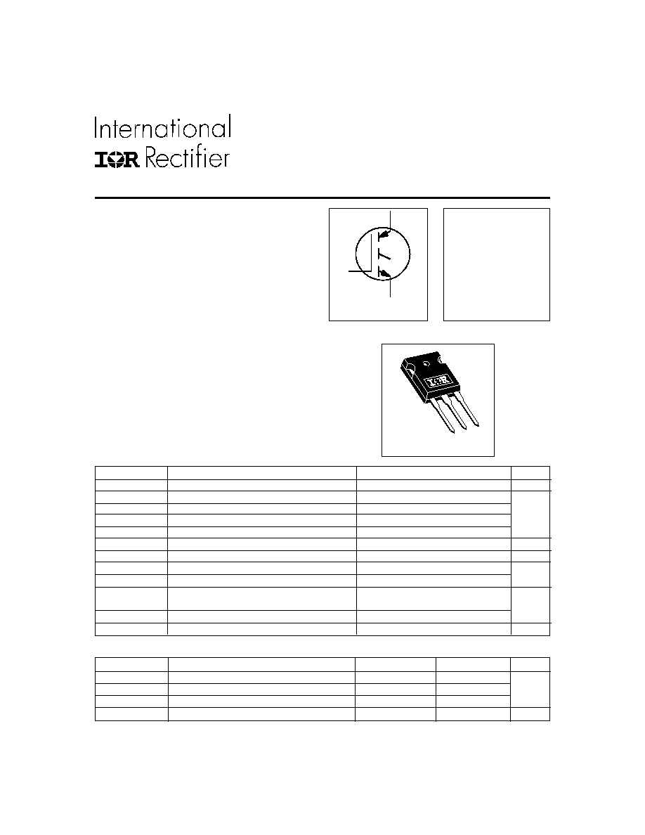
IRG4PC40F
Fast Speed IGBT
INSULATED GATE BIPOLAR TRANSISTOR
PD 91463B
E
C
G
n-channel
TO-247AC
Features
Features
Features
Features
Features
· Fast: Optimized for medium operating
frequencies ( 1-5 kHz in hard switching, >20
kHz in resonant mode).
· Generation 4 IGBT design provides tighter
parameter distribution and higher efficiency than
Generation 3
· Industry standard TO-247AC package
· Generation 4 IGBT's offer highest efficiency available
· IGBT's optimized for specified application conditions
· Designed to be a "drop-in" replacement for equivalent
industry-standard Generation 3 IR IGBT's
Benefits
V
CES
= 600V
V
CE(on) typ.
=
1.50V
@V
GE
= 15V, I
C
= 27A
12/30/00
Parameter
Typ.
Max.
Units
R
JC
Junction-to-Case
0.77
R
CS
Case-to-Sink, Flat, Greased Surface
0.24
°C/W
R
JA
Junction-to-Ambient, typical socket mount
40
Wt
Weight
6 (0.21)
g (oz)
Thermal Resistance
Absolute Maximum Ratings
W
www.irf.com
1
IRG4PC40F
2
www.irf.com
Parameter
Min. Typ. Max. Units
Conditions
Q
g
Total Gate Charge (turn-on)
--
100
150
I
C
= 27A
Q
ge
Gate - Emitter Charge (turn-on)
--
15
23
nC
V
CC
= 400V
See Fig. 8
Q
gc
Gate - Collector Charge (turn-on)
--
35
53
V
GE
= 15V
t
d(on)
Turn-On Delay Time
--
26
--
t
r
Rise Time
--
18
--
T
J
= 25°C
t
d(off)
Turn-Off Delay Time
--
240
360
I
C
= 27A, V
CC
= 480V
t
f
Fall Time
--
170
250
V
GE
= 15V, R
G
= 10
E
on
Turn-On Switching Loss
--
0.37
--
Energy losses include "tail"
E
off
Turn-Off Switching Loss
--
1.81
--
mJ
See Fig. 10, 11, 13, 14
E
ts
Total Switching Loss
--
2.18
2.8
t
d(on)
Turn-On Delay Time
--
25
--
T
J
= 150°C,
t
r
Rise Time
--
21
--
I
C
= 27A, V
CC
= 480V
t
d(off)
Turn-Off Delay Time
--
380
--
V
GE
= 15V, R
G
= 10
t
f
Fall Time
--
310
--
Energy losses include "tail"
E
ts
Total Switching Loss
--
3.9
--
mJ
See Fig. 13, 14
L
E
Internal Emitter Inductance
--
13
--
nH
Measured 5mm from package
C
ies
Input Capacitance
--
2200
--
V
GE
= 0V
C
oes
Output Capacitance
--
140
--
pF
V
CC
= 30V
See Fig. 7
C
res
Reverse Transfer Capacitance
--
29
--
= 1.0MHz
Parameter
Min. Typ. Max. Units
Conditions
V
(BR)CES
Collector-to-Emitter Breakdown Voltage
600
--
--
V
V
GE
= 0V, I
C
= 250µA
V
(BR)ECS
Emitter-to-Collector Breakdown Voltage
T
18
--
--
V
V
GE
= 0V, I
C
= 1.0A
V
(BR)CES
/
T
J
Temperature Coeff. of Breakdown Voltage
--
0.70
--
V/°C
V
GE
= 0V, I
C
= 1.0mA
--
1.50
1.7
I
C
= 27A V
GE
= 15V
V
CE(ON)
Collector-to-Emitter Saturation Voltage
--
1.85
--
I
C
= 49A
See Fig.2, 5
--
1.56
--
I
C
= 27A , T
J
= 150°C
V
GE(th)
Gate Threshold Voltage
3.0
--
6.0
V
CE
= V
GE
, I
C
= 250µA
V
GE(th)
/
T
J
Temperature Coeff. of Threshold Voltage
--
-12
--
mV/°C V
CE
= V
GE
, I
C
= 250µA
g
fe
Forward Transconductance
U
9.2
12
--
S
V
CE
=
100V, I
C
= 27A
--
--
250
V
GE
= 0V, V
CE
= 600V
--
--
2.0
V
GE
= 0V, V
CE
= 10V, T
J
= 25°C
--
--
1000
V
GE
= 0V, V
CE
= 600V, T
J
= 150°C
I
GES
Gate-to-Emitter Leakage Current
--
--
±100
n A
V
GE
= ±20V
Electrical Characteristics @ T
J
= 25°C (unless otherwise specified)
I
CES
Zero Gate Voltage Collector Current
V
µ A
Switching Characteristics @ T
J
= 25°C (unless otherwise specified)
ns
ns
T
Pulse width
80µs; duty factor
0.1%.
U
Pulse width 5.0µs, single shot.
Notes:
Q
Repetitive rating; V
GE
= 20V, pulse width limited by
max. junction temperature. ( See fig. 13b )
R
V
CC
= 80%(V
CES
), V
GE
= 20V, L = 10µH, R
G
= 10
,
(See fig. 13a)
S
Repetitive rating; pulse width limited by maximum
junction temperature.
IRG4PC40F
www.irf.com
3
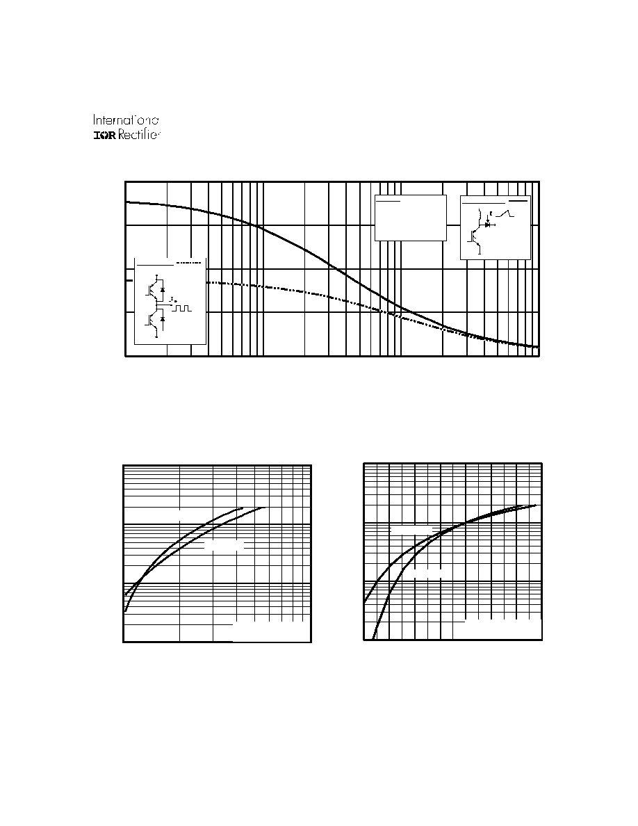
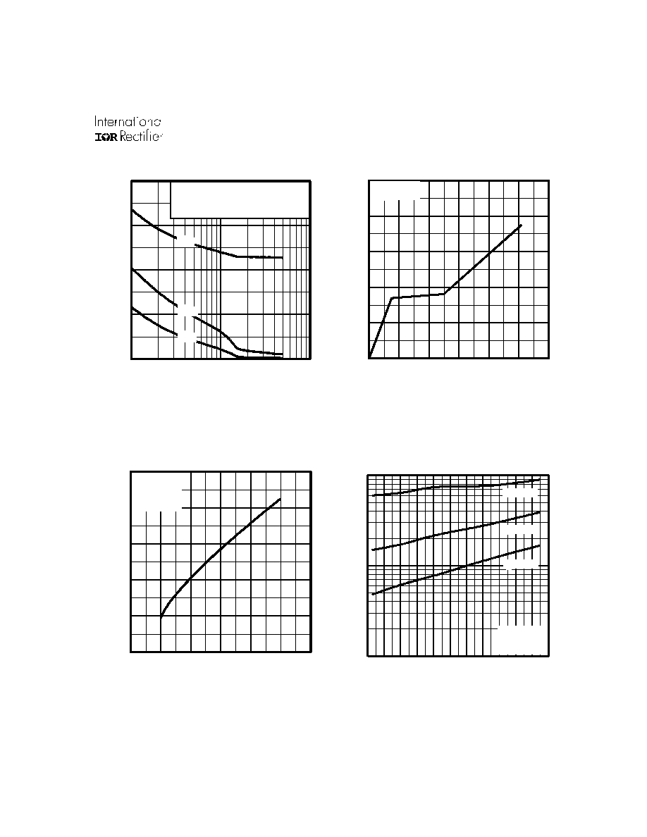
Fig. 1 - Typical Load Current vs. Frequency
(For square wave, I=I
RMS
of fundamental; for triangular wave, I=I
PK
)
Fig. 2 - Typical Output Characteristics
Fig. 3 - Typical Transfer Characteristics
1
1 0
1 0 0
1 0 0 0
5
6
7
8
9
1 0
1 1
1 2
C
I , Collector-to-Emitter Current (A)
G E
T = 25°C
T = 150°C
J
J
V , Gate-to-Emitter Voltage (V)
A
V = 50V
5 µ s P U L S E W I D T H
C C
0
2 0
4 0
6 0
8 0
0 . 1
1
1 0
1 0 0
f, Frequency (kHz)
Load Current (A)
A
60 % o f ra te d
vo lta ge
Ide a l d io de s
S q u a re w a v e :
F o r bo th:
D u ty c y cle : 5 0 %
T = 1 2 5 ° C
T = 9 0 °C
G a te d riv e a s s p e c ifie d
sink
J
T ria ngu la r w a v e:
C lam p vo lta g e:
8 0% o f ra ted
P ow e r D is s ip a tio n = 3 5 W
1
1 0
1 0 0
1 0 0 0
1
1 0
CE
V , C ollec to r-to-E m itter V oltage (V )
T = 15 0°C
T = 25°C
J
J
V = 15V
20µs PU LSE W ID TH
G E
A
I
C
, Collector-to-Emitter Current (A)
IRG4PC40F
4
www.irf.com
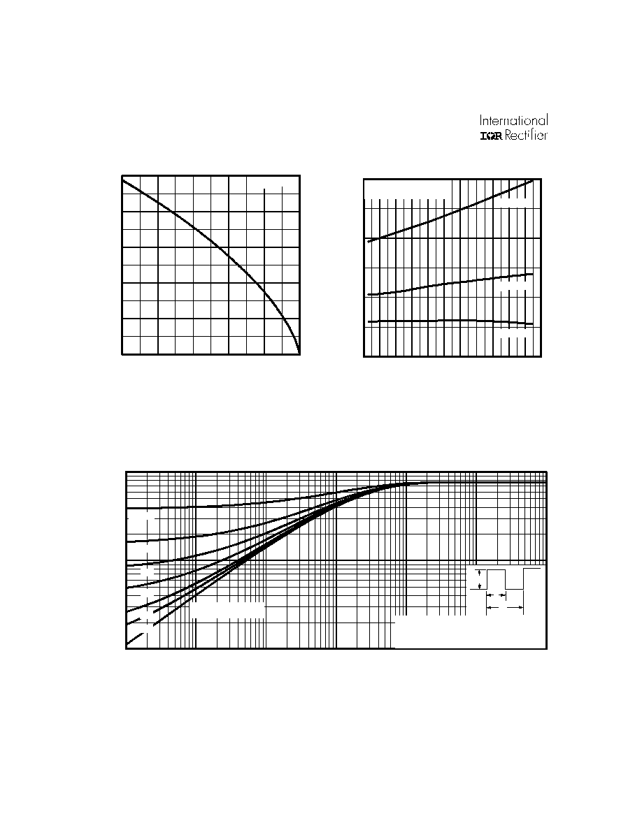
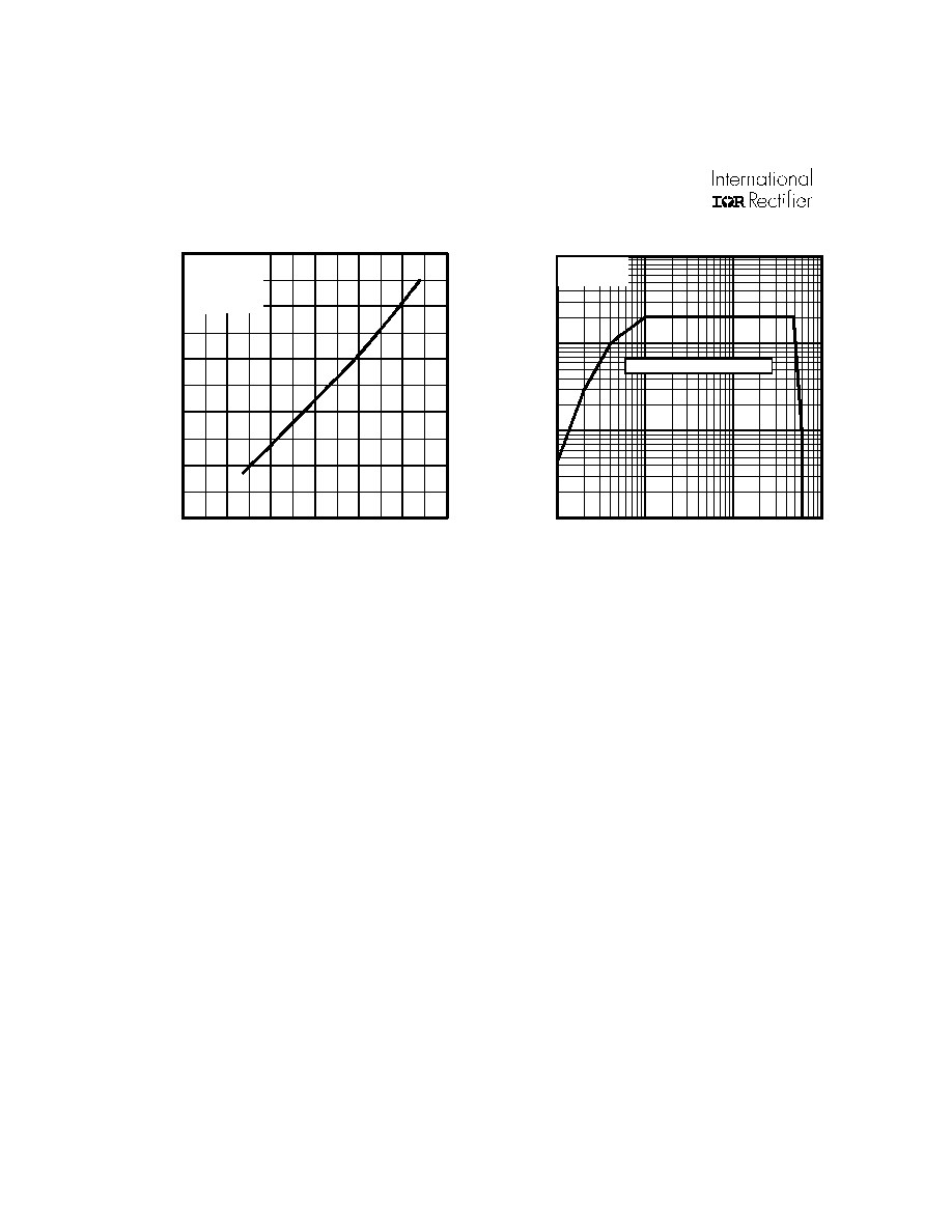
Fig. 6 - Maximum Effective Transient Thermal Impedance, Junction-to-Case
Fig. 5 - Typical Collector-to-Emitter Voltage
vs. Junction Temperature
Fig. 4 - Maximum Collector Current vs. Case
Temperature
0
1 0
2 0
3 0
4 0
5 0
2 5
5 0
7 5
1 0 0
1 2 5
1 5 0
M
a
x
i
m
u
m
DC Co
l
l
e
c
t
o
r
Cu
r
r
e
n
t
(
A
)
T , C ase Tem perature (°C )
C
V = 15 V
G E
1 . 0
1 . 5
2 . 0
2 . 5
- 6 0
- 4 0
- 2 0
0
2 0
4 0
6 0
8 0
1 0 0
1 2 0
1 4 0
1 6 0
CE
V , Collector-to-Emitter Voltage (V)
V = 15V
80µs PULSE WIDTH
G E
A
T , Junction Temperature (°C)
J
I = 54A
I = 27A
I = 14A
C
C
C
0 .0 1
0 .1
1
0 .0 0 0 0 1
0 .0 0 0 1
0 .0 0 1
0 .0 1
0 .1
1
1 0
t , R ectangular Pulse Duration (sec)
1
th
J
C
D = 0 .5 0
0.0 1
0.0 2
0 .05
0.1 0
0.2 0
S IN G LE P UL S E
(T H E R M A L R E S P O NS E )
T
h
e
r
m
a
l
R
e
s
p
ons
e (
Z
)
P
t
2
1
t
D M
N o te s:
1 . D u ty fa c to r D = t / t
2 . P e a k T = P x Z + T
1
2
J
D M
th J C
C
IRG4PC40F
www.irf.com
5
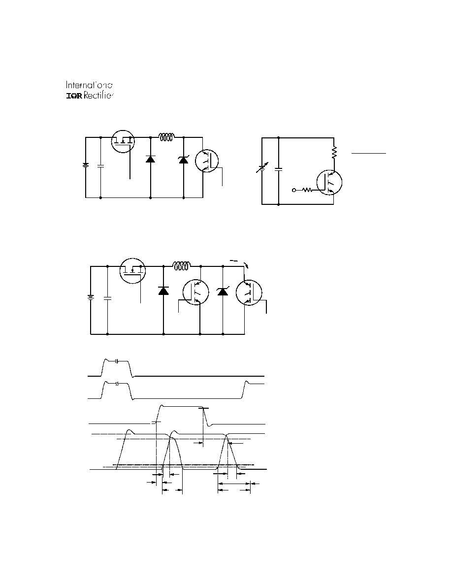
Fig. 10 - Typical Switching Losses vs.
Junction Temperature
Fig. 9 - Typical Switching Losses vs. Gate
Resistance
Fig. 8 - Typical Gate Charge vs.
Gate-to-Emitter Voltage
Fig. 7 - Typical Capacitance vs.
Collector-to-Emitter Voltage
0
4
8
1 2
1 6
2 0
0
2 0
4 0
6 0
8 0
1 0 0
1 2 0
GE
V , Gate-to-Emitter Voltage (V)
g
Q , Total Gate Charge (nC)
A
V = 400V
I = 27A
C E
C
0 . 1
1
1 0
- 6 0
- 4 0
- 2 0
0
2 0
4 0
6 0
8 0
1 0 0
1 2 0
1 4 0
1 6 0
Total Switching Losses (mJ)
A
T , Junction Temperature (°C)
J
R = 10
V = 15V
V = 480V
I = 14A
I = 27A
I = 54A
G
G E
C C
C
C
C
2 . 1 0
2 . 2 0
2 . 3 0
2 . 4 0
2 . 5 0
2 . 6 0
0
1 0
2 0
3 0
4 0
5 0
6 0
A
V = 480V
V = 15V
T = 25°C
I = 27A
R , G ate Resistance
()
C C
G E
J
C
G
Total Switchig Losses (mJ)
0
1 0 0 0
2 0 0 0
3 0 0 0
4 0 0 0
1
1 0
1 0 0
C E
V , Collector-to-Em itter Voltage (V)
A
C
ies
C
res
C
oe s
V
GE
= 0V f = 1 MHz
Cies = Cge + Cgc + Cce SHORTED
Cres = Cce
Coes = Cce + Cgc
C , Capacitance ( pF)
IRG4PC40F
6
www.irf.com
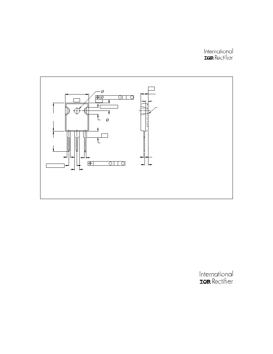
Fig. 12 - Turn-Off SOA
Fig. 11 - Typical Switching Losses vs.
Collector-to-Emitter Current
0
2
4
6
8
1 0
0
1 0
2 0
3 0
4 0
5 0
6 0
C
Total Switching Losses (mJ)
R = 10
T = 150°C
V = 480V
V = 15V
I , Collector-to-Emitter Current (A)
A
G
J
C C
G E
1
1 0
1 0 0
1 0 0 0
1
1 0
1 0 0
1 0 0 0
C
C E
G E
V , Collecto r-to-E m itter V oltage (V )
I
, C
o
l
l
e
c
to
r
-
to
-
E
m
i
t
t
e
r
C
u
r
r
e
n
t (
A
)
S A F E O P E R A TIN G A R E A
V = 2 0V
T = 125 °C
G E
J
IRG4PC40F
www.irf.com
7
480V
4
X
I
C
@
25°C
D .U .T.
5 0V
L
V *
C
Q
R
* Driver s am e ty pe as D .U .T .; Vc = 80% o f V ce (m ax )
* No te: D ue to th e 50V p ow er s up p ly, p ulse w id th a nd ind u ctor
w ill inc rea se to o b ta in ra ted Id.
1 00 0V
Fig. 13a -
Clamped Inductive
Load Test Circuit
Fig. 13b -
Pulsed Collector
Current Test Circuit
4 80 µF
9 60 V
0 - 480V
R
L
=
t=5µ s
d (o n )
t
t
f
t
r
9 0%
t
d (o ff)
1 0%
90 %
10 %
5 %
V
C
I
C
E
o n
E
o ff
ts o n o ff
E = ( E +E )
Q
R
S
Fig. 14b -
Switching Loss
Waveforms
5 0 V
D riv er*
1 00 0V
D .U .T.
I
C
C
V
Q
R
S
L
Fig. 14a -
Switching Loss
Test Circuit
* Driver same type
as D.U.T., VC = 480V
IRG4PC40F
8
www.irf.com
Case Outline and Dimensions TO-247AC
D im e n s io n s in M illim e te rs a n d (In c h e s )
CONFORMS TO JEDEC OUTLINE TO-247AC (TO-3P)
- D -
5 .3 0 ( .2 0 9 )
4 .7 0 ( .1 8 5 )
3 .6 5 (.1 4 3 )
3 .5 5 (.1 4 0 )
2 .5 0 (.0 8 9 )
1 .5 0 (.0 5 9 )
4
3 X
0 .8 0 (.0 3 1 )
0 .4 0 (.0 1 6 )
2 .6 0 ( .1 0 2 )
2 .2 0 ( .0 8 7 )
3 .4 0 (.1 3 3 )
3 .0 0 (.1 1 8 )
3 X
0 .2 5 (.0 1 0 )
M
C A
S
4 .3 0 (.1 7 0 )
3 .7 0 (.1 4 5 )
- C -
2 X
5 .5 0 (.2 17 )
4 .5 0 (.1 77 )
5 .5 0 (.2 1 7)
0 .2 5 (.0 1 0 )
1 .4 0 (.0 5 6 )
1 .0 0 (.0 3 9 )
D
M
M
B
- A -
1 5 .9 0 (.6 2 6 )
1 5 .3 0 (.6 0 2 )
- B -
1
2
3
2 0 .3 0 (.8 0 0 )
1 9 .7 0 (.7 7 5 )
1 4 .8 0 (.5 8 3 )
1 4 .2 0 (.5 5 9 )
2 .4 0 ( .0 9 4 )
2 .0 0 ( .0 7 9 )
2 X
2 X
5 .4 5 (.2 1 5 )
*
N O T E S :
1 D IM E N S IO N S & T O L E R A N C IN G
P E R A N S I Y 14 .5 M , 1 9 8 2 .
2 C O N T R O L L IN G D IM E N S IO N : IN C H .
3 D IM E N S IO N S A R E S H O W N
M ILL IM E T E R S (IN C H E S ).
4 C O N F O R M S T O JE D E C O U T L IN E
T O -2 4 7 A C .
L E A D A S S IG N M E N T S
1 - G A T E
2 - C O L L E C T O R
3 - E M IT T E R
4 - C O L L E C T O R
*
L O N G E R L E A D E D (2 0m m )
V E R S IO N A V A IL A B LE ( T O - 24 7 A D )
T O O R D E R A D D "-E " S U F F IX
T O P A R T N U M B E R
IR WORLD HEADQUARTERS: 233 Kansas St., El Segundo, California 90245, USA Tel: (310) 252-7105
TAC Fax: (310) 252-7903
Visit us at www.irf.com for sales contact information.
Data and specifications subject to change without notice. 12/00