Parameter
Max.
Units
V
CES
Collector-to-Emitter Voltage
600
V
I
C
@ T
C
= 25∞C
Continuous Collector Current
42
I
C
@ T
C
= 100∞C
Continuous Collector Current
25
I
CM
Pulsed Collector Current
Q
84
A
I
LM
Clamped Inductive Load Current
R
84
I
F
@ T
C
= 100∞C
Diode Continuous Forward Current
15
I
FM
Diode Maximum Forward Current
84
t
sc
Short Circuit Withstand Time
10
µs
V
GE
Gate-to-Emitter Voltage
± 20
V
P
D
@ T
C
= 25∞C
Maximum Power Dissipation
160
P
D
@ T
C
= 100∞C
Maximum Power Dissipation
65
T
J
Operating Junction and
-55 to +150
T
STG
Storage Temperature Range
∞C
Soldering Temperature, for 10 sec.
300 (0.063 in. (1.6mm) from case)
Mounting Torque, 6-32 or M3 Screw.
10 lbf∑in (1.1 N∑m)
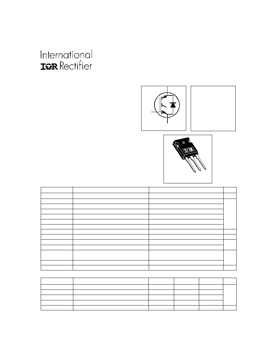
IRG4PC40KD
INSULATED GATE BIPOLAR TRANSISTOR WITH
ULTRAFAST SOFT RECOVERY DIODE
Features
Features
Features
Features
Features
E
G
n-ch an nel
C
V
CES
= 600V
V
CE(on) typ.
=
2.1V
@V
GE
= 15V, I
C
= 25A
Short Circuit Rated
UltraFast IGBT
∑ Short Circuit Rated UltraFast: Optimized for
high operating frequencies >5.0 kHz , and Short
Circuit Rated to 10µs @ 125∞C, V
GE
= 15V
∑ Generation 4 IGBT design provides tighter
parameter distribution and higher efficiency than
Generation 3
∑ IGBT co-packaged with HEXFRED
TM
ultrafast,
ultra-soft-recovery anti-parallel diodes for use in
bridge configurations
∑ Industry standard TO-247AC package
Benefits
∑ Generation 4 IGBTs offer highest efficiencies
available
∑ HEXFRED diodes optimized for performance with
IGBTs. Minimized recovery characteristics require
less/no snubbing
∑ Designed to be a "drop-in" replacement for
equivalent industry-standard Generation 3 IR IGBTs
PD -91584A
TO-247AC
Parameter
Min.
Typ.
Max.
Units
R
JC
Junction-to-Case - IGBT
≠≠≠
≠≠≠
0.77
R
JC
Junction-to-Case - Diode
≠≠≠
≠≠≠
1.7
∞C/W
R
CS
Case-to-Sink, flat, greased surface
≠≠≠
0.24
≠≠≠
R
JA
Junction-to-Ambient, typical socket mount
≠≠≠
≠≠≠
40
Wt
Weight
≠≠≠
6 (0.21)
≠≠≠
g (oz)
Thermal Resistance
Absolute Maximum Ratings
W
4/15/2000
www.irf.com
1
IRG4PC40KD
2
www.irf.com
Parameter
Min. Typ. Max. Units
Conditions
Q
g
Total Gate Charge (turn-on)
--
120
180
I
C
= 25A
Q
ge
Gate - Emitter Charge (turn-on)
--
16
24
nC
V
CC
= 400V
See Fig.8
Q
gc
Gate - Collector Charge (turn-on)
--
51
77
V
GE
= 15V
t
d(on)
Turn-On Delay Time
--
53
--
t
r
Rise Time
--
33
--
T
J
= 25∞C
t
d(off)
Turn-Off Delay Time
--
110
160
I
C
= 25A, V
CC
= 480V
t
f
Fall Time
--
100
150
V
GE
= 15V, R
G
= 10
E
on
Turn-On Switching Loss
--
0.95
--
Energy losses include "tail"
E
off
Turn-Off Switching Loss
--
0.76
--
mJ
See Fig. 9,10,14
E
ts
Total Switching Loss
--
1.71
2.3
t
sc
Short Circuit Withstand Time
10
--
--
µs
V
CC
= 360V, T
J
= 125∞C
V
GE
= 15V, R
G
= 10
, V
CPK
< 500V
t
d(on)
Turn-On Delay Time
--
52
--
T
J
= 150∞C,
t
r
Rise Time
--
37
--
I
C
= 25A, V
CC
= 480V
t
d(off)
Turn-Off Delay Time
--
220
--
V
GE
= 15V, R
G
= 10
t
f
Fall Time
--
140
--
Energy losses include "tail"
E
ts
Total Switching Loss
--
2.67
--
mJ
See Fig. 11,14
L
E
Internal Emitter Inductance
--
13
--
nH
Measured 5mm from package
C
ies
Input Capacitance
--
1600
--
V
GE
= 0V
C
oes
Output Capacitance
--
130
--
pF
V
CC
= 30V
See Fig. 7
C
res
Reverse Transfer Capacitance
--
55
--
= 1.0MHz
t
rr
Diode Reverse Recovery Time
--
42
60
ns
T
J
= 25∞C See Fig.
--
74
120
T
J
= 125∞C 14 I
F
= 15A
I
rr
Diode Peak Reverse Recovery Current
--
4.0
6.0
A
T
J
= 25∞C See Fig.
--
6.5
10
T
J
= 125∞C 15 V
R
= 200V
Q
rr
Diode Reverse Recovery Charge
--
80
180
nC
T
J
= 25∞C See Fig.
--
220
600
T
J
= 125∞C 16 di/dt = 200Aµs
di
(rec)M
/dt
Diode Peak Rate of Fall of Recovery
--
188
--
A/µs
T
J
= 25∞C See Fig.
During t
b
--
160
--
T
J
= 125∞C 17
Parameter
Min. Typ. Max. Units
Conditions
V
(BR)CES
Collector-to-Emitter Breakdown Voltage
S
600
--
--
V
V
GE
= 0V, I
C
= 250µA
V
(BR)CES
/
T
J
Temperature Coeff. of Breakdown Voltage
--
0.46
--
V/∞C
V
GE
= 0V, I
C
= 1.0mA
V
CE(on)
Collector-to-Emitter Saturation Voltage
--
2.10
2.6
I
C
= 25A
V
GE
= 15V
--
2.70
--
V
I
C
= 42A
See Fig. 2, 5
--
2.14
--
I
C
= 25A, T
J
= 150∞C
V
GE(th)
Gate Threshold Voltage
3.0
--
6.0
V
CE
= V
GE
, I
C
= 250µA
V
GE(th)
/
T
J
Temperature Coeff. of Threshold Voltage
--
-13
--
mV/∞C V
CE
= V
GE
, I
C
= 250µA
g
fe
Forward Transconductance
T
7.0
14
--
S
V
CE
= 100V, I
C
= 25A
I
CES
Zero Gate Voltage Collector Current
--
--
250
µA
V
GE
= 0V, V
CE
= 600V
--
--
3500
V
GE
= 0V, V
CE
= 600V, T
J
= 150∞C
V
FM
Diode Forward Voltage Drop
--
1.3
1.7
V
I
C
= 15A
See Fig. 13
--
1.2
1.6
I
C
= 15A, T
J
= 150∞C
I
GES
Gate-to-Emitter Leakage Current
--
--
±100
nA
V
GE
= ±20V
Switching Characteristics @ T
J
= 25∞C (unless otherwise specified)
Electrical Characteristics @ T
J
= 25∞C (unless otherwise specified)
ns
ns

IRG4PC40KD
www.irf.com
3
Fig. 1 - Typical Load Current vs. Frequency
(Load Current = I
RMS
of fundamental)
Fig. 2 - Typical Output Characteristics
Fig. 3 - Typical Transfer Characteristics
1
1 0
1 0 0
5
7
9
1 1
C
I , Collector-to-Emitter Current (A)
G E
T = 25∞C
T = 150∞C
J
J
V , Gate-to-Emitter Voltage (V)
A
V = 50V
5 µ s P U L S E W I D T H
C C
1
10
100
0.1
1
10
V , Collector-to-Emitter Voltage (V)
I , Collector-to-Emitter Current (A)
CE
C
V = 15V
20µs PULSE WIDTH
GE
T = 25 C
J
o
T = 150 C
J
o
0.1
1
10
100
0
5
10
15
20
25
30
f, Frequency (KHz)
LOAD CURRENT (A)
For both:
D uty cy cle : 5 0 %
T = 12 5 ∞C
T = 90 ∞C
G a te d rive a s sp e cifie d
s in k
J
P ow e r Dis sip ation = W
6 0% of rate d
volta ge
I
Id e a l d io d e s
S q u a re w a v e :
35

IRG4PC40KD
4
www.irf.com
Fig. 6 - Maximum Effective Transient Thermal Impedance, Junction-to-Case
Fig. 5 - Typical Collector-to-Emitter Voltage
vs. Junction Temperature
Fig. 4 - Maximum Collector Current vs. Case
Temperature
-60 -40 -20
0
20
40
60
80 100 120 140 160
1.0
2.0
3.0
4.0
5.0
T , Junction Temperature ( C)
V , Collector-to-Emitter Voltage(V)
J
∞
CE
V = 15V
80 us PULSE WIDTH
GE
I = A
12.5
C
I = A
25
C
I = A
50
C
25
50
75
100
125
150
0
10
20
30
40
50
T , Case Temperature ( C)
Maximum DC Collector Current(A)
C
∞
0.01
0.1
1
0.00001
0.0001
0.001
0.01
0.1
1
Notes:
1. Duty factor D = t / t
2. Peak T = P
x Z
+ T
1
2
J
DM
thJC
C
P
t
t
DM
1
2
t , Rectangular Pulse Duration (sec)
Thermal Response (Z )
1
thJC
0.01
0.02
0.05
0.10
0.20
D = 0.50
SINGLE PULSE
(THERMAL RESPONSE)

IRG4PC40KD
www.irf.com
5
0
10
20
30
40
50
1.50
2.00
2.50
3.00
R , Gate Resistance (Ohm)
Total Switching Losses (mJ)
G
V = 480V
V = 15V
T = 25 C
I = 25A
CC
GE
J
C
∞
Fig. 9 - Typical Switching Losses vs. Gate
Resistance
Fig. 10 - Typical Switching Losses vs.
Junction Temperature
-60 -40 -20
0
20
40
60
80 100 120 140 160
0.1
1
10
100
T , Junction Temperature ( C )
Total Switching Losses (mJ)
J
∞
R = Ohm
V = 15V
V = 480V
G
GE
CC
I = A
50
C
I = A
25
C
I = A
12.5
C
R
G
, Gate Resistance
( )
Fig. 7 - Typical Capacitance vs.
Collector-to-Emitter Voltage
Fig. 8 - Typical Gate Charge vs.
Gate-to-Emitter Voltage
0
20
40
60
80
100
120
140
0
4
8
12
16
20
Q , Total Gate Charge (nC)
V , Gate-to-Emitter Voltage (V)
G
GE
V
= 400V
I
= 25A
CC
C
1
10
100
0
500
1000
1500
2000
2500
3000
V , Collector-to-Emitter Voltage (V)
C, Capacitance (pF)
CE
V
C
C
C
=
=
=
=
0V,
C
C
C
f = 1MHz
+ C
+ C
C SHORTED
GE
ies
ge
gc ,
ce
res
gc
oes
ce
gc
Cies
Coes
Cres
10

IRG4PC40KD
6
www.irf.com
1
10
100
1000
1
10
100
1000
V = 20V
T = 125 C
GE
J
o
V , Collector-to-Emitter Voltage (V)
I , Collector-to-Emitter Current (A)
CE
C
SAFE OPERATING AREA
Fig. 11 - Typical Switching Losses vs.
Collector-to-Emitter Current
Fig. 12 - Turn-Off SOA
Fig. 13 - Maximum Forward Voltage Drop vs. Instantaneous Forward Current
0
10
20
30
40
50
0.0
2.0
4.0
6.0
8.0
I , Collector-to-emitter Current (A)
Total Switching Losses (mJ)
C
R = Ohm
T = 150 C
V = 480V
V = 15V
G
J
CC
GE
∞
10
1
1 0
1 0 0
0.8
1.2
1.6
2.0
2.4
F M
F
I
n
s
t
ant
an
eous
F
o
r
w
ar
d C
u
r
r
en
t
-
I
(
A
)
F o rw a rd V o lta g e D ro p - V (V )
T = 1 5 0∞C
T = 1 2 5∞C
T = 2 5∞C
J
J
J
125∞C

IRG4PC40KD
www.irf.com
7
Fig. 14 - Typical Reverse Recovery vs. di
f
/dt
Fig. 15 - Typical Recovery Current vs. di
f
/dt
Fig. 16 - Typical Stored Charge vs. di
f
/dt
Fig. 17 - Typical di
(rec)M
/dt vs. di
f
/dt
0
2 0 0
4 0 0
6 0 0
8 0 0
1 0 0
1 0 0 0
f
d i /d t - (A /µ s)
RR
Q
-
(n
C
)
I = 3 0A
I = 15 A
I = 5 .0A
F
F
F
V = 2 0 0 V
T = 1 2 5 ∞C
T = 2 5 ∞C
R
J
J
1 0 0
1 0 0 0
1 0 0
1 0 0 0
f
di /dt - (A /µs)
d
i
(
r
e
c
)
M
/d
t -
(
A
/
µ
s
)
I = 5 .0A
I = 1 5A
I = 30 A
F
F
F
V = 2 0 0 V
T = 1 2 5 ∞C
T = 2 5 ∞C
R
J
J
2 0
4 0
6 0
8 0
1 0 0
1 0 0
1 0 0 0
f
d i /d t - (A /µ s)
t
-
(
n
s
)
rr
I = 3 0A
I = 1 5A
I = 5 .0 A
F
F
F
V = 2 0 0 V
T = 1 2 5 ∞C
T = 2 5 ∞C
R
J
J
1
1 0
1 0 0
1 0 0
1 0 0 0
f
di /dt - (A /µs)
I
-
(
A
)
IR
R
M
I = 5 .0 A
I = 1 5A
I = 30 A
F
F
F
V = 2 0 0 V
T = 1 2 5 ∞C
T = 2 5 ∞C
R
J
J

IRG4PC40KD
8
www.irf.com
Same ty p e
device as
D .U.T .
D .U .T .
430µF
80%
o f Vce
Fig. 18a -
Test Circuit for Measurement of
I
LM
, E
on
, E
off(diode)
, t
rr
, Q
rr
, I
rr
, t
d(on)
, t
r
, t
d(off)
, t
f
t1
Ic
V ce
t1
t2
9 0 % Ic
1 0 % V c e
td (o ff)
tf
Ic
5 % Ic
t1 + 5 µ S
V c e ic d t
9 0 % V g e
+ V g e
E o ff =
Fig. 18b -
Test Waveforms for Circuit of Fig. 18a, Defining
E
off
, t
d(off)
, t
f
V ce ie d t
t2
t1
5 % V c e
Ic
Ip k
V c c
1 0 % Ic
V c e
t1
t2
D U T V O L T A G E
A N D C U R R E N T
G A T E V O L T A G E D .U .T .
+ V g
1 0 % +V g
9 0 % Ic
tr
td (o n )
D IO D E R E V E R S E
R E C O V E R Y E N E R G Y
tx
E o n =
E re c =
t4
t3
V d id d t
t4
t3
D IO D E R E C O V E R Y
W A V E F O R M S
Ic
V p k
1 0 % V c c
Irr
1 0 % Irr
V cc
trr
Q rr =
trr
tx
id d t
Fig. 18c -
Test Waveforms for Circuit of Fig. 18a,
Defining E
on
, t
d(on)
, t
r
Fig. 18d -
Test Waveforms for Circuit of Fig. 18a,
Defining E
rec
, t
rr
, Q
rr
, I
rr
Vd Ic dt
Vce Ic dt
Ic dt
Vce Ic dt

IRG4PC40KD
www.irf.com
9
V g
G A T E S IG N A L
D E V IC E U N D E R T E S T
C U R R E N T D .U .T .
V O L T A G E IN D .U .T .
C U R R E N T IN D 1
t0
t1
t2
D . U . T .
V *
c
5 0 V
L
1 0 0 0 V
6 0 0 0 µ F
1 0 0 V
Figure 19.
Clamped Inductive Load Test
Circuit
Figure 20.
Pulsed Collector Current
Test Circuit
R
L
=
480V
4 X I
C
@25∞C
0 - 480V
Figure 18e.
Macro Waveforms for
Figure 18a's
Test Circuit

IRG4PC40KD
10
www.irf.com
D im e n s io n s in M illim e te rs a n d (In c h e s )
CO NF O RM S TO J EDEC O U TL IN E TO -2 47AC (T O -3P)
- D -
5 .3 0 (.2 0 9 )
4 .7 0 (.1 8 5 )
3 .6 5 ( .1 4 3 )
3 .5 5 ( .1 4 0 )
2.5 0 ( .0 8 9)
1.5 0 ( .0 5 9)
4
3 X
0 .8 0 ( .0 3 1 )
0 .4 0 ( .0 1 6 )
2 . 6 0 ( .1 0 2 )
2 . 2 0 ( .0 8 7 )
3 . 4 0 ( .1 3 3 )
3 . 0 0 ( .1 1 8 )
3 X
0.2 5 ( .0 1 0 )
M
C A
S
4 .3 0 ( .1 7 0 )
3 .7 0 ( .1 4 5 )
- C -
2X
5.5 0 ( .2 1 7)
4.5 0 ( .1 7 7)
5 .5 0 (.2 17 )
0 .2 5 ( .0 1 0 )
1 .4 0 ( .0 56 )
1 .0 0 ( .0 39 )
D
M
M
B
- A -
1 5 .9 0 ( .6 2 6 )
1 5 .3 0 ( .6 0 2 )
- B -
1
2
3
2 0 .3 0 (.8 0 0 )
1 9 .7 0 (.7 7 5 )
1 4 .8 0 (.5 8 3 )
1 4 .2 0 (.5 5 9 )
2 .4 0 (.0 9 4 )
2 .0 0 (.0 7 9 )
2 X
2 X
5 . 4 5 ( .2 1 5 )
*
N O T E S :
1 D IM E N S IO N S & T O LE R A N C IN G
P E R A N S I Y 14 .5M , 1 98 2 .
2 C O N T R O L L IN G D IM E N S IO N : IN C H .
3 D IM E N S IO N S A R E S H O W N
M IL LIM E T E R S (IN C H E S ).
4 C O N F O R M S T O J E D E C O U T L IN E
T O -2 4 7A C .
L E A D A S S IG N M E N T S
1 - G A T E
2 - C O L L E C T O R
3 - E M IT T E R
4 - C O L L E C T O R
*
LO N G E R LE A D E D (2 0m m )
V E R S IO N A V A IL A B L E (T O -2 47 A D )
T O O R D E R A D D "-E " S U F F IX
T O P A R T N U M B E R
Case Outline -- TO-247AC
Notes:
Q
Repetitive rating: V
GE
=20V; pulse width limited by maximum junction temperature
(figure 20)
R
V
CC
=80%(V
CES
), V
GE
=20V, L=10µH, R
G
= 10
(figure 19)
S
Pulse width
80µs; duty factor
0.1%.
T
Pulse width 5.0µs, single shot.
IR WORLD HEADQUARTERS: 233 Kansas St., El Segundo, California 90245, USA Tel: (310) 252-7105
IR EUROPEAN REGIONAL CENTRE: 439/445 Godstone Rd, Whyteleafe, Surrey CR3 OBL, UK Tel: ++ 44 (0)20 8645 8000
IR CANADA: 15 Lincoln Court, Brampton, Ontario L6T3Z2, Tel: (905) 453 2200
IR GERMANY: Saalburgstrasse 157, 61350 Bad Homburg Tel: ++ 49 (0) 6172 96590
IR ITALY: Via Liguria 49, 10071 Borgaro, Torino Tel: ++ 39 011 451 0111
IR JAPAN: K&H Bldg., 2F, 30-4 Nishi-Ikebukuro 3-Chome, Toshima-Ku, Tokyo 171 Tel: 81 (0)3 3983 0086
IR SOUTHEAST ASIA: 1 Kim Seng Promenade, Great World City West Tower, 13-11, Singapore 237994 Tel: ++ 65 (0)838 4630
IR TAIWAN:16 Fl. Suite D. 207, Sec. 2, Tun Haw South Road, Taipei, 10673 Tel: 886-(0)2 2377 9936
Data and specifications subject to change without notice. 4/00