
IRG4PC50UD
INSULATED GATE BIPOLAR TRANSISTOR WITH
ULTRAFAST SOFT RECOVERY DIODE
Features
Features
Features
Features
Features
E
G
n-ch an nel
C
V
CES
= 600V
V
CE(on) typ.
=
1.65V
@V
GE
= 15V, I
C
= 27A
Parameter
Min.
Typ.
Max.
Units
R
JC
Junction-to-Case - IGBT
------
------
0.64
R
JC
Junction-to-Case - Diode
------
------
0.83
∞C/W
R
CS
Case-to-Sink, flat, greased surface
------
0.24
------
R
JA
Junction-to-Ambient, typical socket mount
-----
-----
40
Wt
Weight
------
6 (0.21)
------
g (oz)
Thermal Resistance
UltraFast CoPack IGBT
12/30/00
Absolute Maximum Ratings
Parameter
Max.
Units
V
CES
Collector-to-Emitter Voltage
600
V
I
C
@ T
C
= 25∞C
Continuous Collector Current
55
I
C
@ T
C
= 100∞C
Continuous Collector Current
27
I
CM
Pulsed Collector Current
Q
220
A
I
LM
Clamped Inductive Load Current
R
220
I
F
@ T
C
= 100∞C
Diode Continuous Forward Current
25
I
FM
Diode Maximum Forward Current
220
V
GE
Gate-to-Emitter Voltage
± 20
V
P
D
@ T
C
= 25∞C
Maximum Power Dissipation
200
P
D
@ T
C
= 100∞C
Maximum Power Dissipation
78
T
J
Operating Junction and
-55 to +150
T
STG
Storage Temperature Range
∞C
Soldering Temperature, for 10 sec.
300 (0.063 in. (1.6mm) from case)
Mounting Torque, 6-32 or M3 Screw.
10 lbf∑in (1.1 N∑m)
∑ UltraFast: Optimized for high operating
frequencies 8-40 kHz in hard switching, >200
kHz in resonant mode
∑ Generation 4 IGBT design provides tighter
parameter distribution and higher efficiency than
Generation 3
∑ IGBT co-packaged with HEXFRED
TM
ultrafast,
ultra-soft-recovery anti-parallel diodes for use in
bridge configurations
∑ Industry standard TO-247AC package
Benefits
∑ Generation 4 IGBT's offer highest efficiencies
available
∑ IGBT's optimized for specific application conditions
∑ HEXFRED diodes optimized for performance with
IGBT's . Minimized recovery characteristics require
less/no snubbing
∑ Designed to be a "drop-in" replacement for equivalent
industry-standard Generation 3 IR IGBT's
PD 91471B
W
TO-247AC
www.irf.com
1

IRG4PC50UD
2
www.irf.com
Parameter
Min. Typ. Max. Units
Conditions
Q
g
Total Gate Charge (turn-on)
----
180
270
I
C
= 27A
Qge
Gate - Emitter Charge (turn-on)
----
25
38
nC
V
CC
= 400V
See Fig. 8
Q
gc
Gate - Collector Charge (turn-on)
----
61
90
V
GE
= 15V
t
d(on)
Turn-On Delay Time
----
46
----
T
J
= 25∞C
t
r
Rise Time
----
25
----
ns
I
C
= 27A, V
CC
= 480V
t
d(off)
Turn-Off Delay Time
----
140
230
V
GE
= 15V, R
G
= 5.0
t
f
Fall Time
----
74
110
Energy losses include "tail" and
E
on
Turn-On Switching Loss
----
0.99
----
diode reverse recovery.
E
off
Turn-Off Switching Loss
----
0.59
----
mJ
See Fig. 9, 10, 11, 18
E
ts
Total Switching Loss
----
1.58
1.9
t
d(on)
Turn-On Delay Time
----
44
----
T
J
= 150∞C, See Fig. 9, 10, 11, 18
t
r
Rise Time
----
27
----
ns
I
C
= 27A, V
CC
= 480V
t
d(off)
Turn-Off Delay Time
----
240
----
V
GE
= 15V, R
G
= 5.0
t
f
Fall Time
----
130
----
Energy losses include "tail" and
E
ts
Total Switching Loss
----
2.3
----
mJ
diode reverse recovery.
L
E
Internal Emitter Inductance
----
13
----
nH
Measured 5mm from package
C
ies
Input Capacitance
----
4000
----
V
GE
= 0V
C
oes
Output Capacitance
----
250
----
pF
V
CC
= 30V
See Fig. 7
C
res
Reverse Transfer Capacitance
----
52
----
= 1.0MHz
t
rr
Diode Reverse Recovery Time
----
50
75
ns
T
J
= 25∞C See Fig.
----
105
160
T
J
= 125∞C 14 I
F
= 25A
I
rr
Diode Peak Reverse Recovery Current
----
4.5
10
A
T
J
= 25∞C See Fig.
----
8.0
15
T
J
= 125∞C 15 V
R
= 200V
Q
rr
Diode Reverse Recovery Charge
----
112
375
nC
T
J
= 25∞C See Fig.
----
420 1200
T
J
= 125∞C 16 di/dt 200A/µs
di
(rec)M
/dt
Diode Peak Rate of Fall of Recovery
----
250
----
A/µs
T
J
= 25∞C
During t
b
----
160
----
T
J
= 125∞C
Parameter
Min. Typ. Max. Units
Conditions
V
(BR)CES
Collector-to-Emitter Breakdown Voltage
S
600
----
----
V
V
GE
= 0V, I
C
= 250µA
V
(BR)CES
/
T
J
Temperature Coeff. of Breakdown Voltage
----
0.60
----
V/∞C
V
GE
= 0V, I
C
= 1.0mA
V
CE(on)
Collector-to-Emitter Saturation Voltage
----
1.65
2.0
I
C
= 27A
V
GE
= 15V
----
2.0
----
V
I
C
= 55A
See Fig. 2, 5
----
1.6
----
I
C
= 27A, T
J
= 150∞C
V
GE(th)
Gate Threshold Voltage
3.0
----
6.0
V
CE
= V
GE
, I
C
= 250µA
V
GE(th)
/
T
J
Temperature Coeff. of Threshold Voltage ----
-13
---- mV/∞C V
CE
= V
GE
, I
C
= 250µA
g
fe
Forward Transconductance
T
16
24
----
S
V
CE
= 100V, I
C
= 27A
I
CES
Zero Gate Voltage Collector Current
----
----
250
µA
V
GE
= 0V, V
CE
= 600V
----
----
6500
V
GE
= 0V, V
CE
= 600V, T
J
= 150∞C
V
FM
Diode Forward Voltage Drop
----
1.3
1.7
V
I
C
= 25A
See Fig. 13
----
1.2
1.5
I
C
= 25A, T
J
= 150∞C
I
GES
Gate-to-Emitter Leakage Current
----
----
±100
nA
V
GE
= ±20V
Switching Characteristics @ T
J
= 25∞C (unless otherwise specified)
Electrical Characteristics @ T
J
= 25∞C (unless otherwise specified)

IRG4PC50UD
www.irf.com
3
Fig. 1 - Typical Load Current vs. Frequency
(Load Current = I
RMS
of fundamental)
Fig. 2 - Typical Output Characteristics
Fig. 3 - Typical Transfer Characteristics
0.1
1
1 0
1 0 0
1 0 0 0
0
1
1 0
C E
C
I
,
C
o
l
l
e
c
to
r-to
-
E
m
i
t
te
r C
u
rr
e
n
t
(
A
)
V , C o lle c to r-to -E m itte r V o lta g e (V )
T = 1 5 0 ∞C
T = 2 5 ∞C
J
J
A
V = 1 5 V
2 0 µ s P U L S E W ID T H
G E
1
1 0
1 0 0
1 0 0 0
4
6
8
1 0
1 2
C
I
, C
o
l
l
e
c
t
o
r
-
t
o
-
E
m
i
t
te
r
C
u
r
r
e
n
t
(
A
)
G E
T = 2 5 ∞C
T = 1 5 0∞C
J
J
V , G a te -to -E m itte r V o lta g e (V )
A
V = 1 0 V
5 µ s P U LS E W ID TH
C C
0
1 0
2 0
3 0
4 0
0 . 1
1
1 0
1 0 0
f, Freq uen cy (kH z)
Loa
d C
u
r
r
e
nt
(A
)
A
6 0 % o f r ate d
v o lta g e
D u ty c ycl e: 5 0%
T = 1 25 ∞C
T = 90 ∞C
G a te d rive a s spe cifi ed
Tu rn -on lo sses inclu de
effe cts o f reve rse re cov ery
sin k
J
P o w e r D issipa tion = 4 0 W

IRG4PC50UD
4
www.irf.com
Fig. 6 - Maximum IGBT Effective Transient Thermal Impedance, Junction-to-Case
Fig. 5 - Typical Collector-to-Emitter Voltage
vs. Junction Temperature
Fig. 4 - Maximum Collector Current vs. Case
Temperature
1 . 0
1 . 5
2 . 0
2 . 5
- 6 0
- 4 0
- 2 0
0
2 0
4 0
6 0
8 0
1 0 0
1 2 0
1 4 0
1 6 0
CE
V
, C
o
l
l
e
c
to
r
-
to
-
E
m
i
tt
e
r
V
o
l
t
a
g
e
(
V
)
V = 1 5V
8 0 µs P U L S E W ID TH
G E
A
T , Ju n c tio n Te m p e ra tu re (∞C )
J
I = 5 4 A
I = 2 7 A
I = 14 A
C
C
C
0
1 0
2 0
3 0
4 0
5 0
6 0
2 5
5 0
7 5
1 0 0
1 2 5
1 5 0
M
a
x
i
m
u
m
D
C
C
o
l
l
e
c
t
o
r
C
u
rre
n
t
(A
)
T , C ase Tem perature (∞C)
C
V = 15 V
G E
0 .0 1
0 .1
1
0 .0 0 0 0 1
0 .0 0 0 1
0 .0 0 1
0 .0 1
0 .1
1
1 0
t , R e c ta n g u la r P u ls e D ura tio n (s e c )
1
th
J
C
D = 0 .5 0
0 .0 1
0 .0 2
0 .0 5
0 .1 0
0 .2 0
S IN G L E P U L S E
( T H E R M A L R E S P O N S E )
T
her
m
a
l
R
e
s
pon
s
e
(
Z
)
P
t
2
1
t
D M
N ote s :
1 . D u ty f ac t or D = t / t
2 . P e a k T = P x Z + T
1
2
J
D M
th J C
C

IRG4PC50UD
www.irf.com
5
Fig. 9 - Typical Switching Losses vs. Gate
Resistance
Fig. 10 - Typical Switching Losses vs.
Junction Temperature
Fig. 8 - Typical Gate Charge vs.
Gate-to-Emitter Voltage
Fig. 7 - Typical Capacitance vs.
Collector-to-Emitter Voltage
0
4
8
1 2
1 6
2 0
0
4 0
8 0
1 2 0
1 6 0
2 0 0
GE
V , Gate-to-Emitter Voltage (V)
g
Q , Total Gate Charge (nC)
A
V = 400V
I = 27A
C E
C
1 . 0
1 . 5
2 . 0
2 . 5
3 . 0
0
1 0
2 0
3 0
4 0
5 0
6 0
G
T
o
t
a
l
S
w
i
t
c
h
i
ng Los
s
e
s
(
m
J
)
A
R , G a te R e s is ta n c e (
)
V = 4 8 0 V
V = 1 5 V
T = 2 5 ∞C
I = 2 7 A
C C
G E
J
C
0 . 1
1
1 0
- 6 0
- 4 0
- 2 0
0
2 0
4 0
6 0
8 0
1 0 0
1 2 0
1 4 0
1 6 0
Total Switching Losses (mJ)
A
T , Junction Temperature (∞C)
J
R = 5.0
V = 15V
V = 480V
I = 54A
I = 27A
I = 14A
G
G E
C C
C
C
C
0
2 0 0 0
4 0 0 0
6 0 0 0
8 0 0 0
1
1 0
1 0 0
C E
C
,
C
apaci
t
ance (
p
F)
V , C o lle c to r-to -E m itte r V o lta g e (V )
A
V = 0 V , f = 1 M H z
C = C + C , C S H O R T E D
C = C
C = C + C
C
ie s
C
res
C
oes
G E
ie s g e g c c e
re s g c
o e s c e g c

IRG4PC50UD
6
www.irf.com
Fig. 11 - Typical Switching Losses vs.
Collector-to-Emitter Current
Fig. 12 - Turn-Off SOA
Fig. 13 - Maximum Forward Voltage Drop vs. Instantaneous Forward Current
1
1 0
1 0 0
0.6
1.0
1.4
1.8
2.2
2.6
F M
F
I
n
s
t
an
t
a
neou
s
F
o
r
w
a
r
d
C
u
r
r
ent
-
I
(
A
)
F o rw a rd V o lta g e D ro p - V (V )
T = 1 50 ∞C
T = 1 25 ∞C
T = 25 ∞C
J
J
J
1
1 0
1 0 0
1 0 0 0
1
1 0
1 0 0
1 0 0 0
C
C E
G E
V , Collecto r-to-E m itter V oltage (V )
I
,
C
o
l
l
e
c
t
o
r
-
t
o
-
E
m
i
t
te
r
C
u
r
r
e
n
t (
A
)
S A FE O P E R A T IN G A R E A
V = 2 0V
T = 125 ∞C
G E
J
0 . 0
2 . 0
4 . 0
6 . 0
8 . 0
0
1 0
2 0
3 0
4 0
5 0
6 0
C
T
o
t
a
l
S
w
i
t
c
h
i
n
g
L
o
ss
e
s
(
m
J)
I , C o lle c to r-to-E m itte r C u rre n t (A )
A
R = 5 .0
T = 1 5 0 ∞C
V = 4 8 0 V
V = 1 5 V
G
J
C C
G E

IRG4PC50UD
www.irf.com
7
Fig. 14 - Typical Reverse Recovery vs. di
f
/dt
Fig. 15 - Typical Recovery Current vs. di
f
/dt
Fig. 16 - Typical Stored Charge vs. di
f
/dt
Fig. 17 - Typical di
(rec)M
/dt vs. di
f
/dt
0
3 0 0
6 0 0
9 0 0
1 2 0 0
1 5 0 0
1 0 0
1 0 0 0
f
d i /d t - (A /µ s )
RR
Q
-
(
n
C
)
I = 1 0A
I = 2 5A
I = 5 0A
F
F
F
V = 2 0 0 V
T = 1 2 5 ∞C
T = 2 5 ∞C
R
J
J
1 0 0
1 0 0 0
1 0 0 0 0
1 0 0
1 0 0 0
f
di /dt - (A /µs)
di
(
r
ec
)
M
/
d
t
-
(
A
/
µ
s
)
I = 5 0A
I = 25 A
I = 10 A
F
F
F
V = 2 0 0 V
T = 1 2 5 ∞C
T = 2 5 ∞C
R
J
J
1
1 0
1 0 0
1 0 0
1 0 0 0
f
d i /d t - (A /µ s)
I
-
(
A
)
IR
R
M
I = 10 A
I = 2 5A
I = 5 0A
F
F
F
V = 2 0 0 V
T = 1 2 5 ∞C
T = 2 5 ∞C
R
J
J
2 0
4 0
6 0
8 0
1 0 0
1 2 0
1 4 0
1 0 0
1 0 0 0
f
di /dt - (A/µs)
t - (ns)
rr
I = 50A
I = 25A
I = 10A
F
F
F
V = 2 0 0 V
T = 1 2 5 ∞ C
T = 2 5 ∞ C
R
J
J
IRG4PC50UD
8
www.irf.com
t1
Ic
V c e
t1
t2
9 0 % Ic
1 0 % V c e
td (o ff)
tf
Ic
5 % Ic
t1 + 5 µ S
V c e ic d t
9 0 % V g e
+ V g e
E o f f =
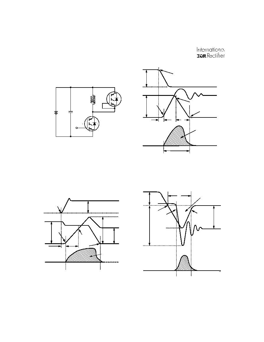
Fig. 18b -
Test Waveforms for Circuit of Fig. 18a, Defining
E
off
, t
d(off)
, t
f
V ce ie d t
t2
t1
5 % V c e
Ic
Ip k
V c c
1 0 % Ic
V c e
t1
t2
D U T V O L T A G E
A N D C U R R E N T
G A T E V O L T A G E D .U .T .
+ V g
1 0 % +V g
9 0 % Ic
tr
td (o n )
D IO D E R E V E R S E
R E C O V E R Y E N E R G Y
tx
E o n =
E re c =
t4
t3
V d id d t
t4
t3
D IO D E R E C O V E R Y
W A V E F O R M S
Ic
V p k
1 0 % V c c
Irr
1 0 % Irr
V cc
trr
Q rr =
trr
tx
id d t
Same ty p e
device as
D .U.T .
D .U .T .
430µF
80%
o f Vce
Fig. 18a -
Test Circuit for Measurement of
I
LM
, E
on
, E
off(diode)
, t
rr
, Q
rr
, I
rr
, t
d(on)
, t
r
, t
d(off)
, t
f
Fig. 18c -
Test Waveforms for Circuit of Fig. 18a,
Defining E
on
, t
d(on)
, t
r
Fig. 18d -
Test Waveforms for Circuit of Fig. 18a,
Defining E
rec
, t
rr
, Q
rr
, I
rr

IRG4PC50UD
www.irf.com
9
V g
G A T E S IG N A L
D E V IC E U N D E R T E S T
C U R R E N T D .U .T .
V O L T A G E IN D .U .T .
C U R R E N T IN D 1
t0
t1
t2
D . U . T .
V *
c
5 0 V
L
1 0 0 0 V
6 0 0 0 µ F
1 0 0 V
Figure 19. Clamped Inductive Load Test
Circuit
Figure 20. Pulsed Collector Current
Test Circuit
R
L
=
480V
4 X I
C
@25∞C
0 - 480V
Figure 18e. Macro Waveforms for
Figure 18a's
Test Circuit

IRG4PC50UD
10
www.irf.com
D im e n s io n s in M illim e te rs a n d (In c h e s )
CO NF O RM S TO J EDEC O U TL IN E TO -2 47AC (T O -3P)
- D -
5 .3 0 (.2 0 9 )
4 .7 0 (.1 8 5 )
3 .6 5 ( .1 4 3 )
3 .5 5 ( .1 4 0 )
2.5 0 ( .0 8 9)
1.5 0 ( .0 5 9)
4
3 X
0 .8 0 ( .0 3 1 )
0 .4 0 ( .0 1 6 )
2 . 6 0 ( .1 0 2 )
2 . 2 0 ( .0 8 7 )
3 . 4 0 ( .1 3 3 )
3 . 0 0 ( .1 1 8 )
3 X
0.2 5 ( .0 1 0 )
M
C A
S
4 .3 0 ( .1 7 0 )
3 .7 0 ( .1 4 5 )
- C -
2X
5.5 0 ( .2 1 7)
4.5 0 ( .1 7 7)
5 .5 0 (.2 17 )
0 .2 5 ( .0 1 0 )
1 .4 0 ( .0 56 )
1 .0 0 ( .0 39 )
D
M
M
B
- A -
1 5 .9 0 ( .6 2 6 )
1 5 .3 0 ( .6 0 2 )
- B -
1
2
3
2 0 .3 0 (.8 0 0 )
1 9 .7 0 (.7 7 5 )
1 4 .8 0 (.5 8 3 )
1 4 .2 0 (.5 5 9 )
2 .4 0 (.0 9 4 )
2 .0 0 (.0 7 9 )
2 X
2 X
5 . 4 5 ( .2 1 5 )
*
N O T E S :
1 D IM E N S IO N S & T O LE R A N C IN G
P E R A N S I Y 14 .5M , 1 98 2 .
2 C O N T R O L L IN G D IM E N S IO N : IN C H .
3 D IM E N S IO N S A R E S H O W N
M IL LIM E T E R S (IN C H E S ).
4 C O N F O R M S T O J E D E C O U T L IN E
T O -2 4 7A C .
L E A D A S S IG N M E N T S
1 - G A T E
2 - C O L L E C T O R
3 - E M IT T E R
4 - C O L L E C T O R
*
LO N G E R LE A D E D (2 0m m )
V E R S IO N A V A IL A B L E (T O -2 47 A D )
T O O R D E R A D D "-E " S U F F IX
T O P A R T N U M B E R
Case Outline TO-247AC
Notes:
Q
Repetitive rating: V
GE
= 20V; pulse width limited by maximum junction temperature
(figure 20)
R
V
CC
= 80%(V
CES
), V
GE
= 20V, L = 10µH, R
G
= 5.0
(figure 19)
S
Pulse width
80µs; duty factor
0.1%.
T
Pulse width 5.0µs, single shot.
IR WORLD HEADQUARTERS: 233 Kansas St., El Segundo, California 90245, USA Tel: (310) 252-7105
TAC Fax: (310) 252-7903
Visit us at www.irf.com for sales contact information.
Data and specifications subject to change without notice. 12/00