 | –≠–ª–µ–∫—Ç—Ä–æ–Ω–Ω—ã–π –∫–æ–º–ø–æ–Ω–µ–Ω—Ç: IRG4PC50W | –°–∫–∞—á–∞—Ç—å:  PDF PDF  ZIP ZIP |

Parameter
Max.
Units
V
CES
Collector-to-Emitter Breakdown Voltage
600
V
I
C
@ T
C
= 25∞C
Continuous Collector Current
55
I
C
@ T
C
= 100∞C
Continuous Collector Current
27
A
I
CM
Pulsed Collector Current
Q
220
I
LM
Clamped Inductive Load Current
R
220
V
GE
Gate-to-Emitter Voltage
± 20
V
E
ARV
Reverse Voltage Avalanche Energy
S
170
mJ
P
D
@ T
C
= 25∞C
Maximum Power Dissipation
200
P
D
@ T
C
= 100∞C
Maximum Power Dissipation
78
T
J
Operating Junction and
-55 to + 150
T
STG
Storage Temperature Range
Soldering Temperature, for 10 seconds
300 (0.063 in. (1.6mm from case )
∞C
Mounting torque, 6-32 or M3 screw.
10 lbf∑in (1.1N∑m)
IRG4PC50W
INSULATED GATE BIPOLAR TRANSISTOR
PD - 91657B
E
C
G
n-channel
TO-247AC
Features
Features
Features
Features
Features
∑ Designed expressly for Switch-Mode Power
Supply and PFC (power factor correction)
applications
∑ Industry-benchmark switching losses improve
efficiency of all power supply topologies
∑ 50% reduction of Eoff parameter
∑ Low IGBT conduction losses
∑ Latest-generation IGBT design and construction offers
tighter parameters distribution, exceptional reliability
∑ Lower switching losses allow more cost-effective
operation than power MOSFETs up to 150 kHz
("hard switched" mode)
∑ Of particular benefit to single-ended converters and
boost PFC topologies 150W and higher
∑ Low conduction losses and minimal minority-carrier
recombination make these an excellent option for
resonant mode switching as well (up to >300 kHz)
Benefits
V
CES
= 600V
V
CE(on) max.
= 2.30V
@V
GE
= 15V, I
C
= 27A
Parameter
Typ.
Max.
Units
R
JC
Junction-to-Case
≠≠≠
0.64
R
CS
Case-to-Sink, Flat, Greased Surface
0.24
≠≠≠
∞C/W
R
JA
Junction-to-Ambient, typical socket mount
≠≠≠
40
Wt
Weight
6 (0.21)
≠≠≠
g (oz)
Thermal Resistance
Absolute Maximum Ratings
W
2/7/2000
www.irf.com
1

IRG4PC50W
2
www.irf.com
Parameter
Min. Typ. Max. Units
Conditions
Q
g
Total Gate Charge (turn-on)
--
180
270
I
C
= 27A
Q
ge
Gate - Emitter Charge (turn-on)
--
24
36
nC
V
CC
= 400V
See Fig.8
Q
gc
Gate - Collector Charge (turn-on)
--
63
95
V
GE
= 15V
t
d(on)
Turn-On Delay Time
--
46
--
t
r
Rise Time
--
33
--
T
J
= 25∞C
t
d(off)
Turn-Off Delay Time
--
120
180
I
C
= 27A, V
CC
= 480V
t
f
Fall Time
--
57
86
V
GE
= 15V, R
G
= 5.0
E
on
Turn-On Switching Loss
--
0.08
--
Energy losses include "tail"
E
off
Turn-Off Switching Loss
--
0.32
--
mJ
See Fig. 9, 10, 14
E
ts
Total Switching Loss
--
0.40
0.5
t
d(on)
Turn-On Delay Time
--
31
--
T
J
= 150∞C,
t
r
Rise Time
--
43
--
I
C
= 27A, V
CC
= 480V
t
d(off)
Turn-Off Delay Time
--
210
--
V
GE
= 15V, R
G
= 5.0
t
f
Fall Time
--
62
--
Energy losses include "tail"
E
ts
Total Switching Loss
--
1.14
--
mJ
See Fig. 10,11, 14
L
E
Internal Emitter Inductance
--
13
--
nH
Measured 5mm from package
C
ies
Input Capacitance
--
3700
--
V
GE
= 0V
C
oes
Output Capacitance
--
260
--
pF
V
CC
= 30V
See Fig. 7
C
res
Reverse Transfer Capacitance
--
68
--
= 1.0MHz
Parameter
Min. Typ. Max. Units
Conditions
V
(BR)CES
Collector-to-Emitter Breakdown Voltage
600
--
--
V
V
GE
= 0V, I
C
= 250µA
V
(BR)CES
Emitter-to-Collector Breakdown Voltage
T
18
--
--
V
V
GE
= 0V, I
C
= 1.0A
V
(BR)CES
/
T
J
Temperature Coeff. of Breakdown Voltage
--
0.41
--
V/∞C
V
GE
= 0V, I
C
= 5.0mA
--
1.93
2.3
I
C
= 27A V
GE
= 15V
V
CE(ON)
Collector-to-Emitter Saturation Voltage
--
2.25
--
I
C
= 55A
See Fig.2, 5
--
1.71
--
I
C
= 27A , T
J
= 150∞C
V
GE(th)
Gate Threshold Voltage
3.0
--
6.0
V
CE
= V
GE
, I
C
= 250µA
V
GE(th)
/
T
J
Temperature Coeff. of Threshold Voltage
--
-11
--
mV/∞C V
CE
= V
GE
, I
C
= 1.0mA
g
fe
Forward Transconductance
U
27
41
--
S
V
CE
= 100 V, I
C
= 27A
--
--
250
V
GE
= 0V, V
CE
= 600V
--
--
2.0
V
GE
= 0V, V
CE
= 10V, T
J
= 25∞C
--
--
5000
V
GE
= 0V, V
CE
= 600V, T
J
= 150∞C
I
GES
Gate-to-Emitter Leakage Current
--
--
±100
nA
V
GE
= ±20V
Electrical Characteristics @ T
J
= 25∞C (unless otherwise specified)
I
CES
Zero Gate Voltage Collector Current
V
µA
Switching Characteristics @ T
J
= 25∞C (unless otherwise specified)
ns
ns
T
Pulse width
80µs; duty factor 0.1%.
U
Pulse width 5.0µs, single shot.
Notes:
Q
Repetitive rating; V
GE
= 20V, pulse width limited by
max. junction temperature. ( See fig. 13b )
R
V
CC
= 80%(V
CES
), V
GE
= 20V, L = 10µH, R
G
= 5.0
,
(See fig. 13a)
S
Repetitive rating; pulse width limited by maximum
junction temperature.

IRG4PC50W
www.irf.com
3
Fig. 1 - Typical Load Current vs. Frequency
(Load Current = I
RMS
of fundamental)
Fig. 2 - Typical Output Characteristics
Fig. 3 - Typical Transfer Characteristics
1
10
100
1000
1
10
V , Collector-to-Emitter Voltage (V)
I , Collector-to-Emitter Current (A)
CE
C
V = 15V
20µs PULSE WIDTH
GE
T = 150 C
J
∞
T = 25 C
J
∞
1
10
100
1000
5
6
7
8
9
10
11
V , Gate-to-Emitter Voltage (V)
I , Collector-to-Emitter Current (A)
GE
C
V = 50V
5µs PULSE WIDTH
CC
T = 150 C
J
∞
T = 25 C
J
∞
0
2 0
4 0
6 0
8 0
1 0 0
0 . 1
1
1 0
1 0 0
1 0 0 0
f, Frequency (kHz)
A
6 0 % o f ra te d
vo l t a g e
Ide a l d io de s
S q u a re wa ve:
F o r b o t h :
D uty cy cle : 5 0%
T = 12 5 ∞C
T = 90 ∞C
G a te drive a s s p e cified
s in k
J
P o w e r D is s ip a t io n = 4 0 W
T ria n g u la r w a v e :
C la m p vo lt a g e :
8 0 % o f ra te d
Load Current ( A )

IRG4PC50W
4
www.irf.com
Fig. 6 - Maximum Effective Transient Thermal Impedance, Junction-to-Case
Fig. 5 - Typical Collector-to-Emitter Voltage
vs. Junction Temperature
Fig. 4 - Maximum Collector Current vs. Case
Temperature
-60 -40 -20
0
20
40
60
80 100 120 140 160
1.0
2.0
3.0
T , Junction Temperature ( C)
V , Collector-to-Emitter Voltage(V)
J
∞
CE
V = 15V
80 us PULSE WIDTH
GE
I = A
54
C
I = A
27
C
I = A
13.5
C
0.001
0.01
0.1
1
0.00001
0.0001
0.001
0.01
0.1
1
Notes:
1. Duty factor D = t / t
2. Peak T = P
x Z
+ T
1
2
J
DM
thJC
C
P
t
t
DM
1
2
t , Rectangular Pulse Duration (sec)
Thermal Response (Z )
1
thJC
0.01
0.02
0.05
0.10
0.20
0.50
SINGLE PULSE
(THERMAL RESPONSE)
25
50
75
100
125
150
0
10
20
30
40
50
60
T , Case Temperature ( C)
Maximum DC Collector Current(A)
C
∞

IRG4PC50W
www.irf.com
5
-60 -40 -20
0
20
40
60
80 100 120 140 160
0.1
1
10
T , Junction Temperature ( C )
Total Switching Losses (mJ)
J
∞
R = Ohm
V = 15V
V = 480V
G
GE
CC
I = A
54
C
I = A
27
C
I = A
13.5
C
0
10
20
30
40
50
0.0
1.0
2.0
3.0
R , Gate Resistance (Ohm)
Total Switching Losses (mJ)
G
V = 480V
V = 15V
T = 25 C
I = 27A
CC
GE
J
C
∞
Fig. 7 - Typical Capacitance vs.
Collector-to-Emitter Voltage
Fig. 8 - Typical Gate Charge vs.
Gate-to-Emitter Voltage
Fig. 9 - Typical Switching Losses vs. Gate
Resistance
Fig. 10 - Typical Switching Losses vs.
Junction Temperature
0
40
80
120
160
200
0
4
8
12
16
20
Q , Total Gate Charge (nC)
V , Gate-to-Emitter Voltage (V)
G
GE
V
= 400V
I
= 27A
CC
C
5.0
1
10
100
0
2000
4000
6000
8000
V , Collector-to-Emitter Voltage (V)
C, Capacitance (pF)
CE
V
C
C
C
=
=
=
=
0V,
C
C
C
f = 1MHz
+ C
+ C
C SHORTED
GE
ies
ge
gc ,
ce
res
gc
oes
ce
gc
Cies
Coes
Cres
R
G
, Gate Resistance (
)

IRG4PC50W
6
www.irf.com
0
10
20
30
40
50
60
0.0
1.0
2.0
3.0
I , Collector-to-emitter Current (A)
Total Switching Losses (mJ)
C
R = Ohm
T = 150 C
V = 480V
V = 15V
G
J
CC
GE
∞
Fig. 11 - Typical Switching Losses vs.
Collector-to-Emitter Current
Fig. 12 - Turn-Off SOA
1
10
100
1000
1
10
100
1000
V = 20V
T = 125 C
GE
J
o
SAFE OPERATING AREA
V , Collector-to-Emitter Voltage (V)
I , Collector-to-Emitter Current (A)
CE
C
5.0
IRG4PC50W
www.irf.com
7
480V
4
X
I
C
@
25∞C
D .U .T.
5 0V
L
V *
C
Q
R
* Driver s am e ty pe as D .U .T .; Vc = 80% o f V ce (m ax )
* No te: D ue to th e 50V p ow er s up p ly, p ulse w id th a nd ind u ctor
w ill inc rea se to o b ta in ra ted Id.
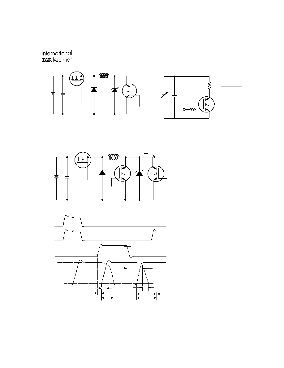
1 00 0V
Fig. 13a -
Clamped Inductive
Load Test Circuit
Fig. 13b -
Pulsed Collector
Current Test Circuit
4 80 µF
9 60 V
0 - 480V
R
L
=
t=5µ s
d (o n )
t
t
f
t
r
90 %
t
d (o ff)
10 %
90 %
1 0%
5 %
V
C
I
C
E
o n
E
o ff
ts o n o ff
E = (E +E )
Q
R
S
Fig. 14b -
Switching Loss
Waveforms
5 0 V
D riv er*
10 00 V
D .U .T.
I
C
C
V
Q
R
S
L
Fig. 14a -
Switching Loss
Test Circuit
* Driver same type
as D.U.T., VC = 480V

IRG4PC50W
8
www.irf.com
Case Outline and Dimensions -- TO-247AC
D im e n s io n s in M illim e te rs a n d (In c h e s )
CONFORMS TO JEDEC OUTLINE TO-247AC (TO-3P)
- D -
5 .3 0 ( .2 0 9 )
4 .7 0 ( .1 8 5 )
3 .6 5 (.1 4 3 )
3 .5 5 (.1 4 0 )
2 .5 0 (.0 8 9 )
1 .5 0 (.0 5 9 )
4
3 X
0 .8 0 (.0 3 1 )
0 .4 0 (.0 1 6 )
2 .6 0 ( .1 0 2 )
2 .2 0 ( .0 8 7 )
3 .4 0 (.1 3 3 )
3 .0 0 (.1 1 8 )
3 X
0 .2 5 (.0 1 0 )
M
C A
S
4 .3 0 (.1 7 0 )
3 .7 0 (.1 4 5 )
- C -
2 X
5 .5 0 (.2 17 )
4 .5 0 (.1 77 )
5 .5 0 (.2 1 7)
0 .2 5 (.0 1 0 )
1 .4 0 (.0 5 6 )
1 .0 0 (.0 3 9 )
D
M
M
B
- A -
1 5 .9 0 (.6 2 6 )
1 5 .3 0 (.6 0 2 )
- B -
1
2
3
2 0 .3 0 (.8 0 0 )
1 9 .7 0 (.7 7 5 )
1 4 .8 0 (.5 8 3 )
1 4 .2 0 (.5 5 9 )
2 .4 0 ( .0 9 4 )
2 .0 0 ( .0 7 9 )
2 X
2 X
5 .4 5 (.2 1 5 )
*
N O T E S :
1 D IM E N S IO N S & T O L E R A N C IN G
P E R A N S I Y 14 .5 M , 1 9 8 2 .
2 C O N T R O L L IN G D IM E N S IO N : IN C H .
3 D IM E N S IO N S A R E S H O W N
M ILL IM E T E R S (IN C H E S ).
4 C O N F O R M S T O JE D E C O U T L IN E
T O -2 4 7 A C .
L E A D A S S IG N M E N T S
1 - G A T E
2 - C O L L E C T O R
3 - E M IT T E R
4 - C O L L E C T O R
*
L O N G E R L E A D E D (2 0m m )
V E R S IO N A V A IL A B LE ( T O - 24 7 A D )
T O O R D E R A D D "-E " S U F F IX
T O P A R T N U M B E R
IR WORLD HEADQUARTERS: 233 Kansas St., El Segundo, California 90245, USA Tel: (310) 252-7105
IR EUROPEAN REGIONAL CENTRE: 439/445 Godstone Rd, Whyteleafe, Surrey CR3 OBL, UK Tel: ++ 44 (0)20 8645 8000
IR CANADA: 15 Lincoln Court, Brampton, Ontario L6T3Z2, Tel: (905) 453 2200
IR GERMANY: Saalburgstrasse 157, 61350 Bad Homburg Tel: ++ 49 (0) 6172 96590
IR ITALY: Via Liguria 49, 10071 Borgaro, Torino Tel: ++ 39 011 451 0111
IR JAPAN: K&H Bldg., 2F, 30-4 Nishi-Ikebukuro 3-Chome, Toshima-Ku, Tokyo 171 Tel: 81 (0)3 3983 0086
IR SOUTHEAST ASIA: 1 Kim Seng Promenade, Great World City West Tower, 13-11, Singapore 237994 Tel: ++ 65 (0)838 4630
IR TAIWAN:16 Fl. Suite D. 207, Sec. 2, Tun Haw South Road, Taipei, 10673 Tel: 886-(0)2 2377 9936
Data and specifications subject to change without notice. 6/00