 | ÐлекÑÑоннÑй компоненÑ: IRG4PH40K | СкаÑаÑÑ:  PDF PDF  ZIP ZIP |
Äîêóìåíòàöèÿ è îïèñàíèÿ www.docs.chipfind.ru
2/7/2000
V
CES
= 1200V
V
CE(on) typ.
= 2.74V
@V
GE
= 15V, I
C
= 15A
Absolute Maximum Ratings
Parameter
Max.
Units
V
CES
Collector-to-Emitter Voltage
1200
V
I
C
@ T
C
= 25°C
Continuous Collector Current
30
I
C
@ T
C
= 100°C
Continuous Collector Current
15
A
I
CM
Pulsed Collector Current
Q
60
I
LM
Clamped Inductive Load Current
R
60
t
sc
Short Circuit Withstand Time
10
µs
V
GE
Gate-to-Emitter Voltage
±20
V
E
ARV
Reverse Voltage Avalanche Energy
S
180
mJ
P
D
@ T
C
= 25°C
Maximum Power Dissipation
160
W
P
D
@ T
C
= 100°C
Maximum Power Dissipation
65
T
J
Operating Junction and
-55 to +150
T
STG
Storage Temperature Range
°C
Soldering Temperature, for 10 sec.
300 (0.063 in. (1.6mm) from case)
Mounting torque, 6-32 or M3 screw.
10 lbf·in (1.1N·m)
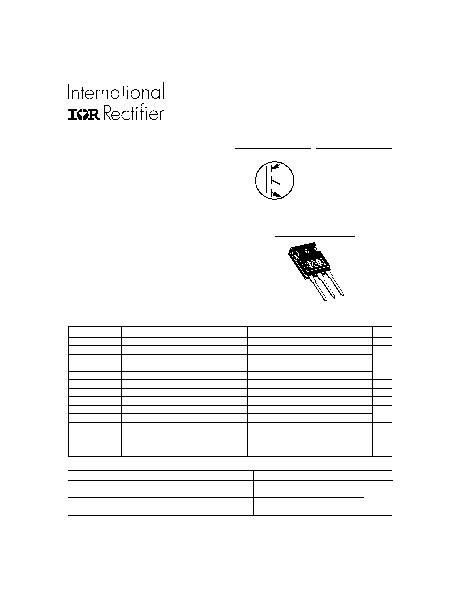
IRG4PH40K
Short Circuit Rated
UltraFast IGBT
INSULATED GATE BIPOLAR TRANSISTOR
PD - 91578B
Parameter
Typ.
Max.
Units
R
JC
Junction-to-Case
0.77
R
CS
Case-to-Sink, Flat, Greased Surface
0.24
°C/W
R
JA
Junction-to-Ambient, typical socket mount
40
Wt
Weight
6 (0.21)
g (oz)
Thermal Resistance
TO-247AC
Features
Features
Features
Features
Features
Benefits
E
C
G
n-channel
· High short circuit rating optimized for motor control,
t
sc
=10µs, V
CC
= 720V , T
J
= 125°C,
V
GE
= 15V
· Combines low conduction losses with high
switching speed
· Latest generation design provides tighter parameter
distribution and higher efficiency than previous
generations
· As a Freewheeling Diode we recommend our
HEXFRED
TM
ultrafast, ultrasoft recovery diodes for
minimum EMI / Noise and switching losses in the
Diode and IGBT
· Latest generation 4 IGBT's offer highest power
density motor controls possible
· This part replaces the IRGPH40K and IRGPH40M
devices
www.irf.com
1
IRG4PH40K
2
www.irf.com
Parameter
Min. Typ. Max. Units
Conditions
V
(BR)CES
Collector-to-Emitter Breakdown Voltage
1200
--
--
V
V
GE
= 0V, I
C
= 250µA
V
(BR)ECS
Emitter-to-Collector Breakdown Voltage
T
18
--
--
V
V
GE
= 0V, I
C
= 1.0A
V
(BR)CES
/
T
J
Temperature Coeff. of Breakdown Voltage
--
0.37
--
V/°C
V
GE
= 0V, I
C
= 1.0mA
--
2.54
--
I
C
= 10A
--
2.74
3.4
I
C
= 15A V
GE
= 15V
--
3.29
--
I
C
= 30A
See Fig.2, 5
--
2.53
--
I
C
= 15A , T
J
= 150°C
V
GE(th)
Gate Threshold Voltage
3.0
--
6.0
V
CE
= V
GE
, I
C
= 250µA
V
GE(th)
/
T
J
Temperature Coeff. of Threshold Voltage
--
-3.3
--
mV/°C V
CE
= V
GE
, I
C
= 250µA
g
fe
Forward Transconductance
U
8.0
12
--
S
V
CE
= 100 V, I
C
= 15A
--
--
250
V
GE
= 0V, V
CE
= 1200V
I
CES
Zero Gate Voltage Collector Current
--
--
2.0
µA
V
GE
= 0V, V
CE
= 10V, T
J
= 25°C
--
--
3000
V
GE
= 0V, V
CE
= 1200V, T
J
= 150°C
I
GES
Gate-to-Emitter Leakage Current
--
--
±100
nA
V
GE
= ±20V
Electrical Characteristics @ T
J
= 25°C (unless otherwise specified)
V
V
CE(ON)
Collector-to-Emitter Saturation Voltage
Details of note
Q through U are on the last page
Parameter
Min. Typ. Max. Units
Conditions
Q
g
Total Gate Charge (turn-on)
--
94
140
I
C
= 15A
Q
ge
Gate - Emitter Charge (turn-on)
--
14
22
nC
V
CC
= 400V
See Fig.8
Q
gc
Gate - Collector Charge (turn-on)
--
37
55
V
GE
= 15V
t
d(on)
Turn-On Delay Time
--
30
--
t
r
Rise Time
--
22
--
T
J
= 25°C
t
d(off)
Turn-Off Delay Time
--
200
300
I
C
= 15A, V
CC
= 960V
t
f
Fall Time
--
150
230
V
GE
= 15V, R
G
= 10
E
on
Turn-On Switching Loss
--
0.73
--
Energy losses include "tail"
E
off
Turn-Off Switching Loss
--
1.66
--
mJ
See Fig. 9,10,14
E
ts
Total Switching Loss
--
2.39
2.9
t
sc
Short Circuit Withstand Time
10
--
--
µs
V
CC
= 720V, T
J
= 125°C
V
GE
= 15V, R
G
= 10
t
d(on)
Turn-On Delay Time
--
29
--
T
J
= 150°C,
t
r
Rise Time
--
24
--
I
C
= 15A, V
CC
= 960V
t
d(off)
Turn-Off Delay Time
--
870
--
V
GE
= 15V, R
G
= 10
t
f
Fall Time
--
330
--
Energy losses include "tail"
E
ts
Total Switching Loss
--
4.93
--
mJ
See Fig. 10,11,14
E
on
Turn-On Switching Loss
--
0.37
--
T
J
= 25°C
, V
GE
= 15V, R
G
= 10
E
off
Turn-Off Switching Loss
--
0.89
--
mJ
I
C
= 10A, V
CC
= 960V
E
ts
Total Switching Loss
--
1.26
--
Energy losses include "tail"
L
E
Internal Emitter Inductance
--
13
--
nH
Measured 5mm from package
C
ies
Input Capacitance
--
1600
--
V
GE
= 0V
C
oes
Output Capacitance
--
77
--
pF
V
CC
= 30V
See Fig. 7
C
res
Reverse Transfer Capacitance
--
26
--
= 1.0MHz
Switching Characteristics @ T
J
= 25°C (unless otherwise specified)
ns
ns
IRG4PH40K
www.irf.com
3
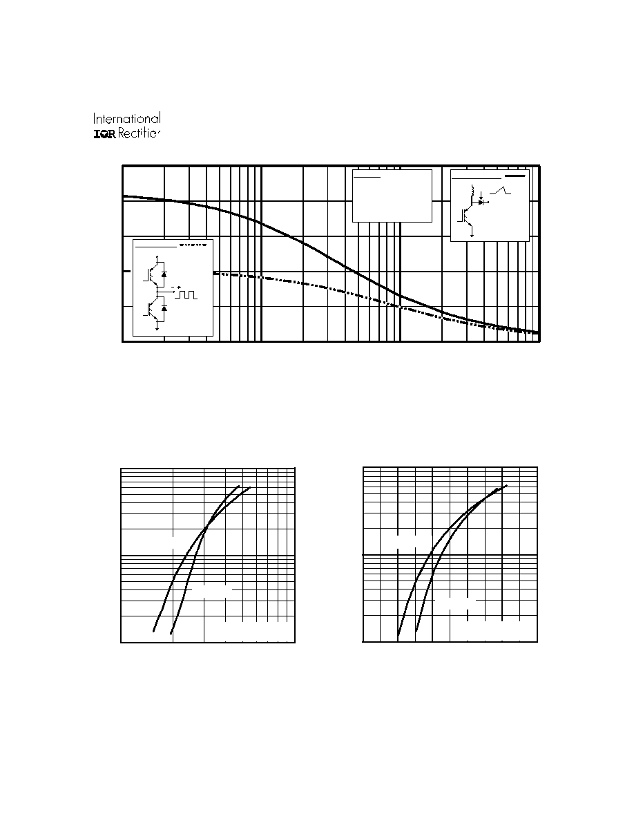
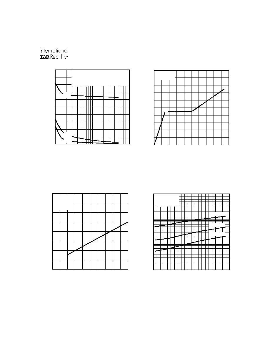
Fig. 1 - Typical Load Current vs. Frequency
(Load Current = I
RMS
of fundamental)
Fig. 2 - Typical Output Characteristics
Fig. 3 - Typical Transfer Characteristics
1
10
100
1
10
V , Collector-to-Emitter Voltage (V)
I , Collector-to-Emitter Current (A)
CE
C
V = 15V
20µs PULSE WIDTH
GE
T = 25 C
J
°
T = 150 C
J
°
0
1 0
2 0
3 0
4 0
5 0
0 . 1
1
1 0
1 0 0
f, Frequency (kHz)
A
6 0 % o f ra t e d
v o lt a g e
I
Id e al d io de s
S q u a re wave :
F o r b o t h :
D u ty c yc le : 50 %
T = 12 5 ° C
T = 9 0 °C
G a te drive as sp e c ifie d
s in k
J
T ria n g u la r w a ve :
I
C la m p vo l ta g e :
8 0 % o f r a te d
P o w e r D is s ip a t io n = 3 5 W
Load Current ( A )
1
10
100
4
6
8
10
12
14
V , Gate-to-Emitter Voltage (V)
I , Collector-to-Emitter Current (A)
GE
C
V = 50V
5µs PULSE WIDTH
CC
T = 25 C
J
°
T = 150 C
J
°
IRG4PH40K
4
www.irf.com
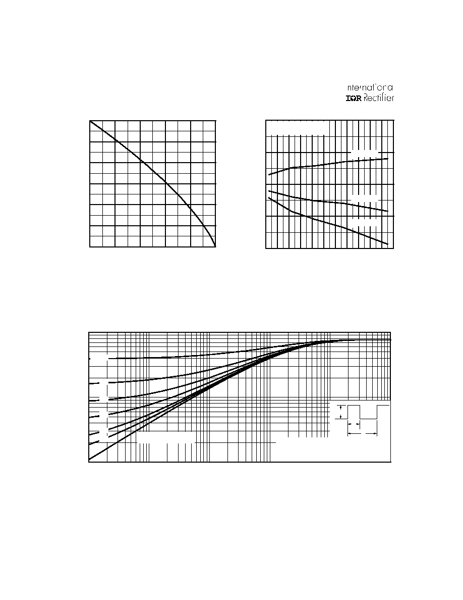
Fig. 6 - Maximum Effective Transient Thermal Impedance, Junction-to-Case
Fig. 5 - Typical Collector-to-Emitter Voltage
vs. Junction Temperature
Fig. 4 - Maximum Collector Current vs. Case
Temperature
25
50
75
100
125
150
0
5
10
15
20
25
30
T , Case Temperature ( C)
Maximum DC Collector Current(A)
C
°
0.01
0.1
1
0.00001
0.0001
0.001
0.01
0.1
1
Notes:
1. Duty factor D = t / t
2. Peak T = P
x Z
+ T
1
2
J
DM
thJC
C
P
t
t
DM
1
2
t , Rectangular Pulse Duration (sec)
Thermal Response (Z )
1
thJC
0.01
0.02
0.05
0.10
0.20
D = 0.50
SINGLE PULSE
(THERMAL RESPONSE)
-60 -40 -20
0
20
40
60
80 100 120 140 160
2.0
2.5
3.0
3.5
4.0
T , Junction Temperature ( C)
V , Collector-to-Emitter Voltage(V)
J
°
CE
V = 15V
80 us PULSE WIDTH
GE
I = A
30
C
I = A
15
C
I = A
7.5
C
IRG4PH40K
www.irf.com
5
0
10
20
30
40
50
2.0
2.5
3.0
3.5
4.0
R , Gate Resistance (Ohm)
Total Switching Losses (mJ)
G
V = 960V
V = 15V
T = 25 C
I = 15A
CC
GE
J
C
°
Fig. 7 - Typical Capacitance vs.
Collector-to-Emitter Voltage
Fig. 8 - Typical Gate Charge vs.
Gate-to-Emitter Voltage
Fig. 9 - Typical Switching Losses vs. Gate
Resistance
Fig. 10 - Typical Switching Losses vs.
Junction Temperature
0
20
40
60
80
100
0
4
8
12
16
20
Q , Total Gate Charge (nC)
V , Gate-to-Emitter Voltage (V)
G
GE
V
= 400V
I
= 15A
CC
C
-60 -40 -20
0
20
40
60
80 100 120 140 160
0.1
1
10
100
T , Junction Temperature ( C )
Total Switching Losses (mJ)
J
°
R = Ohm
V = 15V
V = 960V
G
GE
CC
I = A
30
C
I = A
15
C
I = A
7.5
C
10
1
10
100
0
500
1000
1500
2000
2500
V , Collector-to-Emitter Voltage (V)
C, Capacitance (pF)
CE
V
C
C
C
=
=
=
=
0V,
C
C
C
f = 1MHz
+ C
+ C
C SHORTED
GE
ies
ge
gc ,
ce
res
gc
oes
ce
gc
Cres
Coes
Cies
R
G
, Gate Resistance (
)