Äîêóìåíòàöèÿ è îïèñàíèÿ www.docs.chipfind.ru
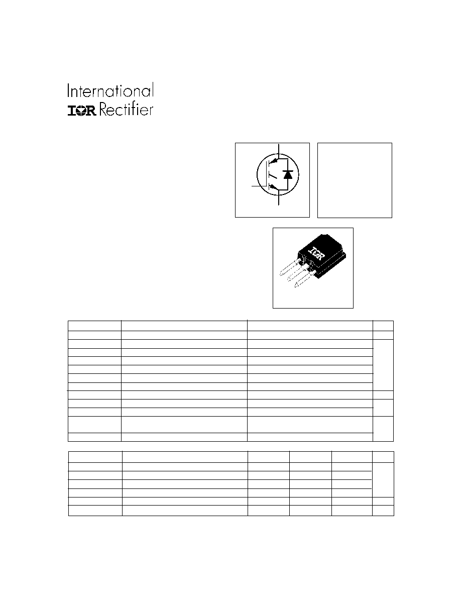
IRG4PSC71UD
INSULATED GATE BIPOLAR TRANSISTOR WITH
ULTRAFAST SOFT RECOVERY DIODE
Features
E
G
n-cha n ne l
C
V
CES
= 600V
V
CE(on) typ.
= 1.67V
@V
GE
= 15V, I
C
= 60A
UltraFast CoPack IGBT
5/12/99
Absolute Maximum Ratings
Parameter
Max.
Units
V
CES
Collector-to-Emitter Voltage
600
V
I
C
@ T
C
= 25°C
Continuous Collector Current
85
I
C
@ T
C
= 100°C
Continuous Collector Current
60
I
CM
Pulsed Collector Current
200
A
I
LM
Clamped Inductive Load Current
200
I
F
@ T
C
= 100°C
Diode Continuous Forward Current
60
I
FM
Diode Maximum Forward Current
350
V
GE
Gate-to-Emitter Voltage
± 20
V
P
D
@ T
C
= 25°C
Maximum Power Dissipation
350
P
D
@ T
C
= 100°C
Maximum Power Dissipation
140
T
J
Operating Junction and
-55 to +150
T
STG
Storage Temperature Range
°C
Soldering Temperature, for 10 sec.
300 (0.063 in. (1.6mm) from case)
Benefits
PD - 91682A
W
www.irf.com
1
· Generation 4 IGBT design provides tighter
parameter distribution and higher efficiency
(minimum switching and conduction losses) than
prior generations
· IGBT co-packaged with HEXFRED ultrafast, ultrasoft
recovery anti-parallel diodes for use in bridge
configurations
· Industry-benchmark Super-247 package with
higher power handling capability compared to
same footprint TO-247
· Creepage distance increased to 5.35mm
·
Generation 4 IGBT's offer highest efficiencies
available
· Maximum power density, twice the power
handling of TO-247, less space than TO-264
· IGBTs optimized for specific application conditions
· HEXFRED diodes optimized for performance with IGBTs
· Cost and space saving in designs that require
multiple, paralleled IGBTs
SUPER - 247
Parameter
Min.
Typ.
Max.
Units
R
JC
Junction-to-Case - IGBT
0.36
R
JC
Junction-to-Case - Diode
0.69
°C/W
R
CS
Case-to-Sink, flat, greased surface
0.24
R
JA
Junction-to-Ambient, typical socket mount
38
Recommended Clip Force
20.0(2.0)
N (kgf)
Weight
6 (0.21)
g (oz)
Thermal Resistance\ Mechanical
IRG4PSC71UD
2
www.irf.com
Parameter
Min. Typ. Max. Units
Conditions
Q
g
Total Gate Charge (turn-on)
340
520
I
C
= 60A
Qge
Gate - Emitter Charge (turn-on)
44
66
nC
V
CC
= 400V
See Fig. 8
Q
gc
Gate - Collector Charge (turn-on)
160
240
V
GE
= 15V
t
d(on)
Turn-On Delay Time
90
T
J
= 25°C
t
r
Rise Time
94
ns
I
C
= 60A, V
CC
= 480V
t
d(off)
Turn-Off Delay Time
245
368
V
GE
= 15V, R
G
= 5.0
t
f
Fall Time
110
167
Energy losses include "tail" and
E
on
Turn-On Switching Loss
3.26
diode reverse recovery.
E
off
Turn-Off Switching Loss
2.27
mJ
See Fig. 9, 10, 11, 18
E
ts
Total Switching Loss
5.53
7.2
t
d(on)
Turn-On Delay Time
91
T
J
= 150°C, See Fig. 9, 10, 11, 18
t
r
Rise Time
88
ns
I
C
= 60A, V
CC
= 480V
t
d(off)
Turn-Off Delay Time
353
V
GE
= 15V, R
G
= 5.0
t
f
Fall Time
150
Energy losses include "tail" and
E
ts
Total Switching Loss
7.1
mJ
diode reverse recovery.
L
E
Internal Emitter Inductance
13
nH
Measured 5mm from package
C
ies
Input Capacitance
7500
V
GE
= 0V
C
oes
Output Capacitance
720
pF
V
CC
= 30V
See Fig. 7
C
res
Reverse Transfer Capacitance
93
= 1.0MHz
t
rr
Diode Reverse Recovery Time
82
120
T
J
= 25°C See Fig.
140
210
T
J
= 125°C 14 I
F
= 60A
I
rr
Diode Peak Reverse Recovery Current
8.2
12
T
J
= 25°C See Fig.
13
20
T
J
= 125°C 15 V
R
= 200V
Q
rr
Diode Reverse Recovery Charge
364
546
T
J
= 25°C See Fig.
1084 1625
T
J
= 125°C 16 di/dt = 200A/µs
di
(rec)M
/dt
Diode Peak Rate of Fall of Recovery
328
T
J
= 25°C See Fig.
During t
b
266
T
J
= 125°C 17
Parameter
Min. Typ. Max. Units
Conditions
V
(BR)CES
Collector-to-Emitter Breakdown Voltage
600
V
V
GE
= 0V, I
C
= 250µA
V
(BR)CES
/
T
J
Temperature Coeff. of Breakdown Voltage
0.39
V/°C
V
GE
= 0V, I
C
= 10mA
V
CE(on)
Collector-to-Emitter Saturation Voltage
1.67
2.0
I
C
= 60A
V
GE
= 15V
1.95
I
C
= 100A
See Fig. 2, 5
1.71
I
C
= 60A, T
J
= 150°C
V
GE(th)
Gate Threshold Voltage
3.0
6.0
V
CE
= V
GE
, I
C
= 250µA
V
GE(th)
/
T
J
Temperature Coeff. of Threshold Voltage
-13
mV/°C V
CE
= V
GE
, I
C
= 1.5mA
g
fe
Forward Transconductance
47
70
S
V
CE
= 50V, I
C
= 60A
I
CES
Zero Gate Voltage Collector Current
500
µA
V
GE
= 0V, V
CE
= 600V
13
mA
V
GE
= 0V, V
CE
= 600V, T
J
= 150°C
V
FM
Diode Forward Voltage Drop
1.4
1.7
I
C
= 60A
See Fig. 13
1.3
I
C
= 60A, T
J
= 150°C
I
GES
Gate-to-Emitter Leakage Current
±100
nA
V
GE
= ±20V
Switching Characteristics @ T
J
= 25°C (unless otherwise specified)
Electrical Characteristics @ T
J
= 25°C (unless otherwise specified)
V
V
ns
A
nC
A/µs
IRG4PSC71UD
www.irf.com
3
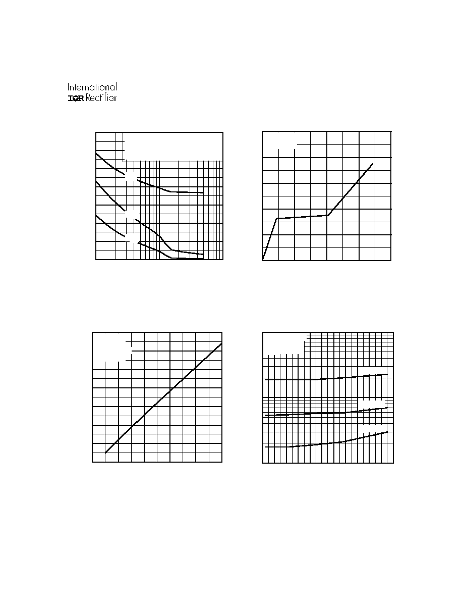
Fig. 1 - Typical Load Current vs. Frequency
(Load Current = I
RMS
of fundamental)
Fig. 2 - Typical Output Characteristics
Fig. 3 - Typical Transfer Characteristics
0.1
1
10
100
0
20
40
60
80
f, Frequency (KHz)
LOAD CURRENT (A)
F or b oth:
D uty c y c le : 50 %
T = 12 5° C
T = 90 °C
G a te d riv e a s s pe c ified
sink
J
P o w e r D is s ip a tio n = W
6 0% o f ra te d
vo lta ge
I
Id e a l d io d es
S q u a re w a v e :
58
1
10
100
1000
5
6
7
8
9
10
V , Gate-to-Emitter Voltage (V)
I , Collector-to-Emitter Current (A)
GE
C
V = 50V
5µs PULSE WIDTH
CC
T = 150 C
J
°
T = 25 C
J
°
1
10
100
1000
1.0
1.5
2.0
2.5
3.0
3.5
V , Collector-to-Emitter Voltage (V)
I , Collector Current (A)
CE
C
V = 15V
80µs PULSE WIDTH
GE
T = 25 C
J
°
T = 150 C
J
°
Ic , Collector-to-Emitter Current (A)
IRG4PSC71UD
4
www.irf.com
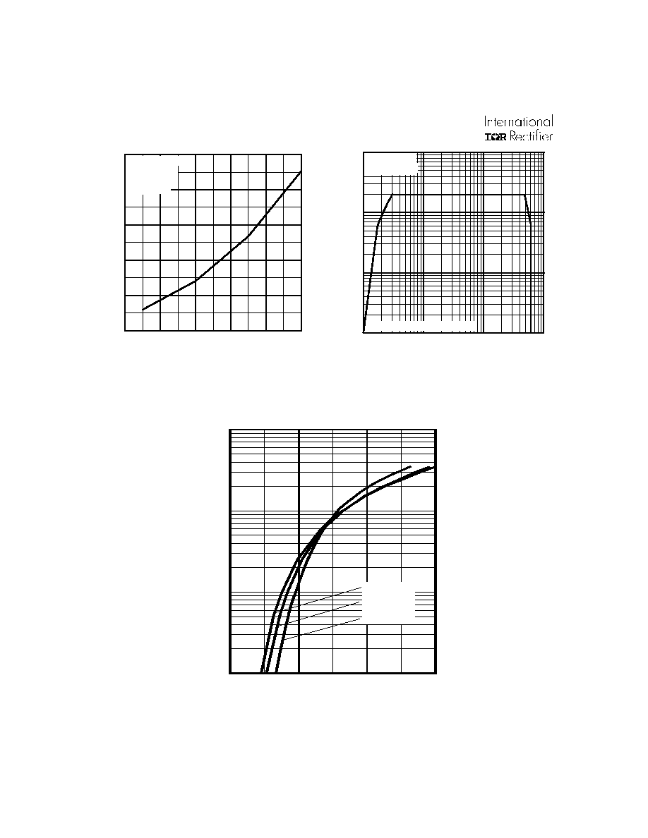
Fig. 6 - Maximum IGBT Effective Transient Thermal Impedance, Junction-to-Case
Fig. 5 - Typical Collector-to-Emitter Voltage
vs. Junction Temperature
Fig. 4 - Maximum Collector Current vs. Case
Temperature
-60 -40 -20
0
20
40
60
80 100 120 140 160
1.0
2.0
3.0
T , Junction Temperature ( C)
V , Collector-to-Emitter Voltage(V)
J
°
CE
V = 15V
80 us PULSE WIDTH
GE
I = A
120
C
I = A
60
C
I = A
30
C
Maximum DC Collector Current (A)
0.01
0.1
1
0 . 0 0 0 1
0 . 0 0 1
0 . 0 1
0.1
1
1 0
1 0 0
1
t , R e cta n g u la r P u ls e D u ra tio n (s e c)
A
D = 0 .5 0
0 .20
0 .1 0
0 .05
0 .0 2
0.0 1
S IN G L E P U L S E
(T H E R M A L R E S P O N S E )
P
t2
1
t
DM
Notes:
1. Duty factor D = t / t
2. Peak T = P x Z + T
1
2
J
DM
thJC
C
Thermal Response (Z
thJC
)
0
2 0
4 0
6 0
8 0
1 0 0
2 5
5 0
7 5
1 0 0
1 2 5
1 5 0
T , C a s e T e m p e ra tu re (°C )
C
A
V = 1 5 V
L IM IT E D B Y P A C K A G E
G E
IRG4PSC71UD
www.irf.com
5
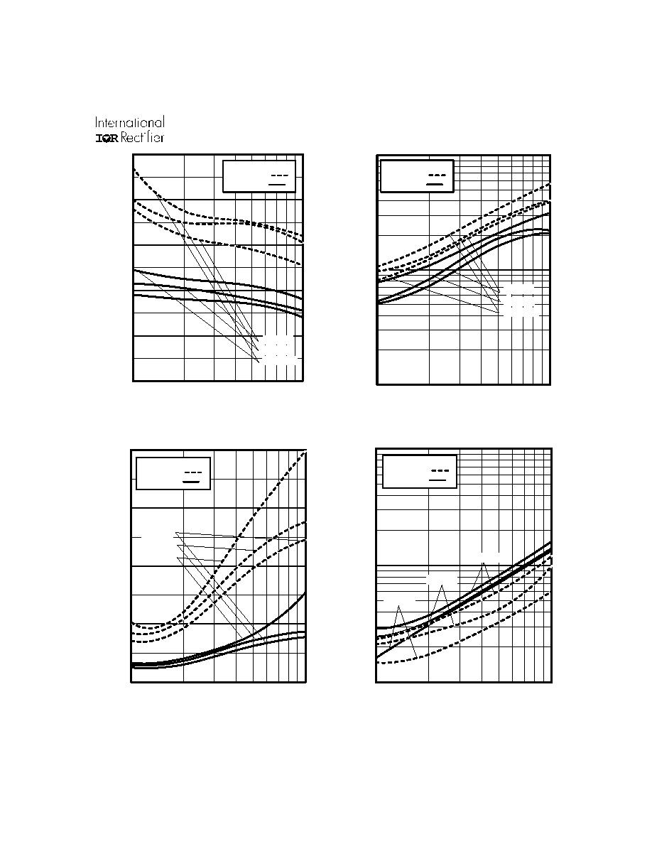
Fig. 9 - Typical Switching Losses vs. Gate
Resistance
Fig. 10 - Typical Switching Losses vs.
Junction Temperature
Fig. 8 - Typical Gate Charge vs.
Gate-to-Emitter Voltage
Fig. 7 - Typical Capacitance vs.
Collector-to-Emitter Voltage
1
10
100
0
2000
4000
6000
8000
10000
12000
14000
V , Collector-to-Emitter Voltage (V)
C, Capacitance (pF)
CE
V
C
C
C
=
=
=
=
0V,
C
C
C
f = 1MHz
+ C
+ C
C SHORTED
GE
ies
ge
gc ,
ce
res
gc
oes
ce
gc
C
ies
C
oes
C
res
0
10
20
30
40
50
5.0
6.0
7.0
8.0
9.0
10.0
11.0
12.0
R , Gate Resistance
Total Switching Losses (mJ)
G
V = 480V
V = 15V
T = 25 C
I = 60A
CC
GE
J
C
°
0
100
200
300
400
0
4
8
12
16
20
Q , Total Gate Charge (nC)
V , Gate-to-Emitter Voltage (V)
G
GE
V
= 400V
I
= 60A
CC
C
R
G
, Gate Resistance
( )
-60 -40 -20
0
20
40
60
80 100 120 140 160
1
10
100
T , Junction Temperature ( C )
Total Switching Losses (mJ)
J
°
R = 5.0Ohm
V = 15V
V = 480V
G
GE
CC
I = A
120
C
I = A
60
C
I = A
30
C
5.0
IRG4PSC71UD
6
www.irf.com
Fig. 13 - Maximum Forward Voltage Drop vs. Instantaneous Forward Current
Instantaneous forward current - I
F
(A)
Fig. 11 - Typical Switching Losses vs.
Collector-to-Emitter Current
Fig. 12 - Turn-Off SOA
1
1 0
1 0 0
1 0 0 0
0 . 0
1 . 0
2 . 0
3 . 0
F M
F o r w a r d V o l ta g e D r o p - V ( V )
T = 1 5 0 ° C
T = 1 2 5 ° C
T = 2 5 ° C
J
J
J
20
40
60
80
100
120
0
5
10
15
20
25
I , Collector Current (A)
Total Switching Losses (mJ)
C
R = 5.0Ohm
T = 150 C
V = 480V
V = 15V
G
J
CC
GE
°
1
10
100
1000
1
10
100
1000
V = 20V
T = 125 C
GE
J
o
SAFE OPERATING AREA
V , Collector-to-Emitter Voltage (V)
I , Collector Current (A)
CE
C
IRG4PSC71UD
www.irf.com
7
Fig. 14 - Typical Reverse Recovery vs. di
f
/dt
Fig. 15 - Typical Recovery Current vs. di
f
/dt
Fig. 16 - Typical Stored Charge vs. di
f
/dt
Fig. 17 - Typical di
(rec)M
/dt vs. di
f
/dt
0
4 0
8 0
1 20
1 60
2 00
10 0
1 0 0 0
f
d i /d t - (A /µ s)
I = 3 0 A
I = 6 0 A
I = 1 2 0 A
F
F
F
R
J
J
V = 2 0 0 V
T = 1 2 5 °C
T = 2 5 °C
1
10
10 0
10 0
1 0 00
f
d i /d t - (A /µ s )
I = 3 0 A
I = 6 0 A
I = 1 2 0 A
F
F
F
R
J
J
V = 2 0 0 V
T = 1 2 5 °C
T = 2 5 °C
0
1 0 0 0
2 0 0 0
3 0 0 0
4 0 0 0
1 0 0
1 0 0 0
f
d i /d t - (A /µ s)
I = 3 0 A
I = 6 0 A
I = 1 2 0 A
F
F
F
R
J
J
V = 2 0 0 V
T = 1 2 5 °C
T = 2 5 ° C
1 0 0
1 0 0 0
1 0 0 0 0
1 0 0
1 0 0 0
f
d i /d t - (A /µ s)
I = 3 0A
I = 60 A
I = 12 0 A
F
F
F
R
J
J
V = 2 0 0 V
T = 1 2 5 °C
T = 2 5 °C
di (rec) M/dt-
(A /µs)
Irr-
(
A
)
trr-
(nC)
Qrr- (nC)
IRG4PSC71UD
8
www.irf.com
Sam e type
device as
D .U.T.
D .U .T.
430µF
80%
of Vce
Fig. 18a -
Test Circuit for Measurement of
I
LM
, E
on
, E
off(diode)
, t
rr
, Q
rr
, I
rr
, t
d(on)
, t
r
, t
d(off)
, t
f
t1
Ic
V ce
t1
t2
9 0 % Ic
1 0 % V ce
td (o ff)
tf
Ic
5 % Ic
t1 +5 µ S
V ce ic d t
9 0 % V g e
+V g e
E o ff =
Fig. 18b -
Test Waveforms for Circuit of Fig. 18a, Defining
E
off
, t
d(off)
, t
f
V c e ie d t
t2
t1
5 % V c e
Ic
Ip k
V c c
1 0 % Ic
V c e
t1
t2
D U T V O L T A G E
A N D C U R R E N T
G A T E V O L T A G E D .U .T .
+V g
1 0 % + V g
9 0 % Ic
tr
td (o n )
D IO D E R E V E R S E
R E C O V E R Y E N E R G Y
tx
E o n =
E re c =
t4
t3
V d id d t
t4
t3
D IO D E R E C O V E R Y
W A V E F O R M S
Ic
V p k
1 0 % V c c
Irr
1 0 % Irr
V c c
trr
Q rr =
trr
tx
id d t
Fig. 18c -
Test Waveforms for Circuit of Fig. 18a,
Defining E
on
, t
d(on)
, t
r
Fig. 18d -
Test Waveforms for Circuit of Fig. 18a,
Defining E
rec
, t
rr
, Q
rr
, I
rr
Vc Ic dt
Vce Ic dt
Ic dt
Vce Ic dt
IRG4PSC71UD
www.irf.com
9
V g
G A T E S IG N A L
D E V IC E U N D E R T E S T
C U R R E N T D .U .T .
V O L T A G E IN D .U .T .
C U R R E N T IN D 1
t0
t1
t2
D.U.T.
V *
c
5 0 V
L
1 000 V
60 0 0 µ F
1 00 V
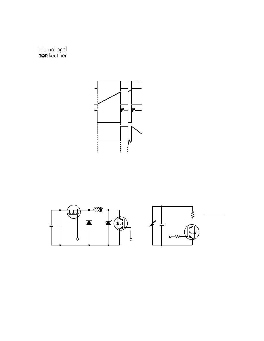
Figure 19. Clamped Inductive Load Test Circuit
Figure 20. Pulsed Collector Current
Test Circuit
R
L
=
480V
4 X I
C
@25°C
0 - 480V
Figure 18e. Macro Waveforms for
Figure 18a's
Test Circuit
IRG4PSC71UD
10
www.irf.com
Notes:
Repetitive rating: V
GE
=20V; pulse width limited by maximum junction
temperature (figure 20)
V
CC
=80%(V
CES
), V
GE
=20V, L=10µH, R
G
= 5.0
(figure 19)
Pulse width
80µs; duty factor
0.1%
Pulse width 5.0µs, single shot
Current limited by the package, (Die current = 100A)
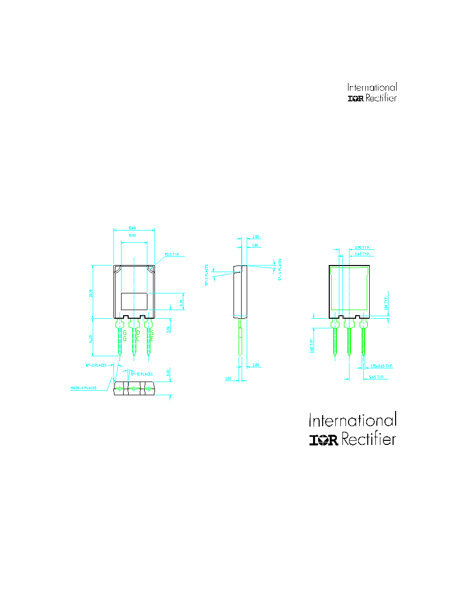
Case Outline and Dimensions -- Super-247
Dimensions are shown in millimeters
WORLD HEADQUARTERS: 233 Kansas St., El Segundo, California 90245, Tel: (310) 322 3331
IR GREAT BRITAIN: Hurst Green, Oxted, Surrey RH8 9BB, UK Tel: ++ 44 1883 732020
IR CANADA: 15 Lincoln Court, Brampton, Ontario L6T3Z2, Tel: (905) 453 2200
IR GERMANY: Saalburgstrasse 157, 61350 Bad Homburg Tel: ++ 49 6172 96590
IR ITALY: Via Liguria 49, 10071 Borgaro, Torino Tel: ++ 39 11 451 0111
IR FAR EAST: K&H Bldg., 2F, 30-4 Nishi-Ikebukuro 3-Chome, Toshima-Ku, Tokyo Japan 171 Tel: 81 3 3983 0086
IR SOUTHEAST ASIA: 1 Kim Seng Promenade, Great World City West Tower, 13-11, Singapore 237994 Tel: ++ 65 838 4630
IR TAIWAN:16 Fl. Suite D. 207, Sec. 2, Tun Haw South Road, Taipei, 10673, Taiwan Tel: 886-2-2377-9936
http://www.irf.com/ Data and specifications subject to change without notice. 5/99