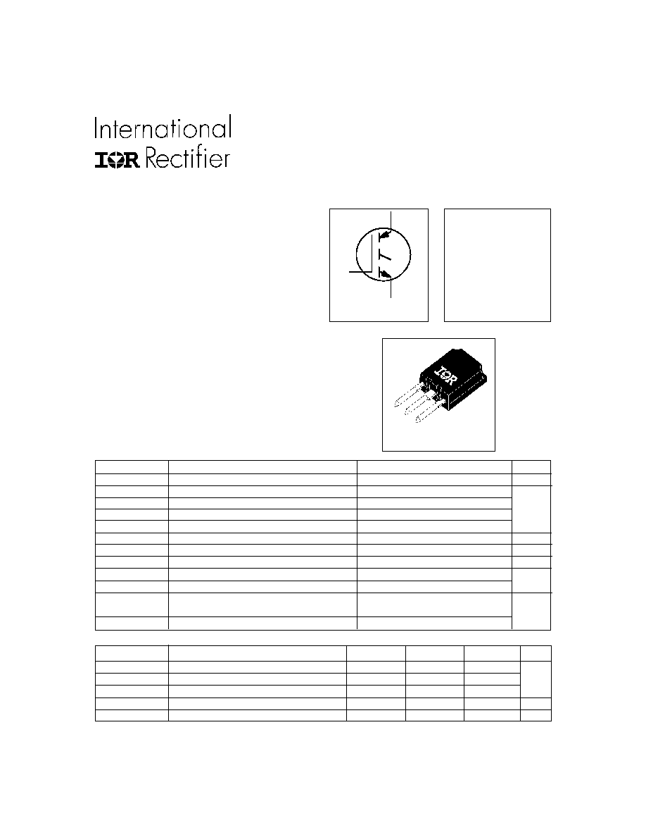
IRG4PSH71K
Short Circuit Rated
UltraFast IGBT
INSULATED GATE BIPOLAR TRANSISTOR
PD - 91687A
E
C
G
n-channel
PRELIMINARY
Features
∑ Hole-less clip/pressure mount package compatible
with TO-247 and TO-264, with reinforced pins
∑ High short circuit rating IGBTs, optimized for
motorcontrol
∑ Minimum switching losses combined with low
conduction losses
∑ Tightest parameter distribution
∑ Creepage distance increased to 5.35mm
∑ Highest current rating IGBT
∑ Maximum power density, twice the power
handling of the TO-247, less space than TO-264
Benefits
V
CES
= 1200V
V
CE(on) typ.
= 2.97V
@V
GE
= 15V, I
C
= 42A
V
CES
Collector-to-Emitter Breakdown Voltage
1200
V
I
C
@ T
C
= 25∞C
Continuous Collector Current
78
I
C
@ T
C
= 100∞C
Continuous Collector Current
42
I
CM
Pulsed Collector Current
156
I
LM
Clamped Inductive Load Current
156
t
SC
Short Circuit Withstand Time
10
µs
V
GE
Gate-to-Emitter Voltage
± 20
V
E
ARV
Reverse Voltage Avalanche Energy
170
mJ
P
D
@ T
C
= 25∞C
Maximum Power Dissipation
350
P
D
@ T
C
= 100∞C
Maximum Power Dissipation
140
T
J
Operating Junction and
-55 to + 150
T
STG
Storage Temperature Range
Soldering Temperature, for 10 seconds
300 (0.063 in. (1.6mm from case )
∞C
Absolute Maximum Ratings
W
5/11/99
www.irf.com
1
SUPER - 247
Parameter
Min.
Typ.
Max.
Units
R
JC
Junction-to-Case
≠≠≠
≠≠≠
0.36
R
CS
Case-to-Sink, flat, greased surface
≠≠≠
0.24
≠≠≠
∞C/W
R
JA
Junction-to-Ambient, typical socket mount
≠≠≠
≠≠≠
38
Recommended Clip Force
20.0(2.0)
≠≠≠
≠≠≠
N (kgf)
Weight
≠≠≠
6 (0.21)
≠≠≠
g (oz)
Thermal Resistance\ Mechanical
Parameter
Max.
Units
A

IRG4PSH71K
2
www.irf.com
Parameter
Min. Typ. Max. Units
Conditions
V
(BR)CES
Collector-to-Emitter Breakdown Voltage
1200
≠≠≠
≠≠≠
V
V
GE
= 0V, I
C
= 250µA
V
(BR)ECS
Emitter-to-Collector Breakdown Voltage
18
≠≠≠
≠≠≠
V
V
GE
= 0V, I
C
= 1.0A
V
(BR)CES
/
T
J
Temperature Coeff. of Breakdown Voltage ≠≠≠
1.1
≠≠≠
V/∞C
V
GE
= 0V, I
C
= 10mA
≠≠≠
2.97
3.9
I
C
= 42A V
GE
= 15V
V
CE(ON)
Collector-to-Emitter Saturation Voltage
≠≠≠
3.44
≠≠≠
I
C
= 78A
See Fig.2, 5
≠≠≠
2.60
≠≠≠
I
C
= 42A , T
J
= 150∞C
V
GE(th)
Gate Threshold Voltage
3.0
≠≠≠
6.0
V
CE
= V
GE
, I
C
= 250µA
V
GE(th)
/
T
J
Temperature Coeff. of Threshold Voltage
≠≠≠
-12
≠≠≠
mV/∞C V
CE
= V
GE
, I
C
= 1.5mA
g
fe
Forward Transconductance
25
38
≠≠≠
S
V
CE
= 50V, I
C
= 42A
≠≠≠
≠≠≠
500
V
GE
= 0V, V
CE
= 1200V
≠≠≠
≠≠≠
2.0
V
GE
= 0V, V
CE
= 10V, T
J
= 25∞C
≠≠≠
≠≠≠
5.0
mA
V
GE
= 0V, V
CE
= 1200V, T
J
= 150∞C
I
GES
Gate-to-Emitter Leakage Current
≠≠≠
≠≠≠ ±100
nA
V
GE
= ±20V
Electrical Characteristics @ T
J
= 25∞C (unless otherwise specified)
I
CES
Zero Gate Voltage Collector Current
V
µA
Switching Characteristics @ T
J
= 25∞C (unless otherwise specified)
Pulse width
80µs; duty factor
0.1%
Pulse width 5.0µs, single shot
Repetitive rating; V
GE
= 20V, pulse width limited by
max. junction temperature. ( See fig. 13b )
V
CC
= 80%(V
CES
), V
GE
= 20V, L =
10µH, R
G
= 5.0
,
(See fig. 13a)
Repetitive rating; pulse width limited by maximum
junction temperature
Parameter
Min. Typ. Max. Units
Conditions
Q
g
Total Gate Charge (turn-on)
--
410
610
I
C
= 42A
Q
ge
Gate - Emitter Charge (turn-on)
--
47
70
nC
V
CC
= 400V
See Fig.8
Q
gc
Gate - Collector Charge (turn-on)
--
145
220
V
GE
= 15V
t
d(on)
Turn-On Delay Time
--
45
--
t
r
Rise Time
--
38
--
T
J
= 25∞C
t
d(off)
Turn-Off Delay Time
--
220
340
I
C
= 42A, V
CC
= 960V
t
f
Fall Time
--
160
250
V
GE
= 15V, R
G
= 5.0
E
on
Turn-On Switching Loss
--
2.35
--
Energy losses include "tail"
E
off
Turn-Off Switching Loss
--
3.14
--
mJ
See Fig. 9,10,14
E
ts
Total Switching Loss
--
5.49
8.3
t
sc
Short Circuit Withstand Time
10
--
--
µs
V
CC
= 720V, T
J
= 125∞C
V
GE
= 20V, R
G
= 5.0
t
d(on)
Turn-On Delay Time
--
42
--
T
J
= 150∞C
t
r
Rise Time
--
41
--
I
C
= 42A, V
CC
= 960V
t
d(off)
Turn-Off Delay Time
--
460
--
V
GE
= 15V, R
G
= 5.0
t
f
Fall Time
--
250
--
Energy losses include "tail"
E
ts
Total Switching Loss
--
11.5
--
mJ
See Fig. 10,11,14
L
E
Internal Emitter Inductance
--
13
--
nH
Measured 5mm from package
C
ies
Input Capacitance
--
5770
--
V
GE
= 0V
C
oes
Output Capacitance
--
400
--
pF
V
CC
= 30V
See Fig. 7
C
res
Reverse Transfer Capacitance
--
100
--
= 1.0MHz
ns
ns
Notes:

IRG4PSH71K
www.irf.com
3
Fig. 1 - Typical Load Current vs. Frequency
(For square wave, I=I
RMS
of fundamental; for triangular wave, I=I
PK
)
Fig. 2 - Typical Output Characteristics
Fig. 3 - Typical Transfer Characteristics
1
10
100
1000
1.0
2.0
3.0
4.0
5.0
V , Collector-to-Emitter Voltage (V)
I , Collector Current (A)
CE
C
V = 15V
80µs PULSE WIDTH
GE
T = 150 C
J
∞
T = 25 C
J
∞
Ic , Collector-to-Emitter Current (A)
1
10
100
1000
5
6
7
8
9
10
11
V , Gate-to-Emitter Voltage (V)
I , Collector-to-Emitter Current (A)
GE
C
V = 50V
5µs PULSE WIDTH
CC
T = 150 C
J
∞
T = 25 C
J
∞
0
20
40
60
80
0.1
1
10
100
f, F req ue nc y (kH z )
Loa
d C
u
r
r
ent
(
A
)
A
60% of rated
voltage
Ideal diodes
Square wave:
For both:
Duty cycle: 50%
T = 125∞C
T = 90∞C
Gate drive as specified
sink
J
Triangular wave:
Clamp voltage:
80% of rated
Power Dissipation = 58W

IRG4PSH71K
4
www.irf.com
Fig. 6 - Maximum Effective Transient Thermal Impedance, Junction-to-Case
Fig. 5 - Collector-to-Emitter Voltage vs.
Junction Temperature
Fig. 4 - Maximum Collector Current vs. Case
Temperature
0 . 0 1
0 . 1
1
0 . 0 0 0 1
0 . 0 0 1
0 . 0 1
0 . 1
1
1 0
1 0 0
1
t , R e ctang ular P ulse D uratio n (sec)
A
D = 0 .50
0 .20
0 .1 0
0.05
0.0 2
0.01
S IN G L E P U L S E
(T HE R M A L R E S P O N S E )
P
t2
1
t
DM
Notes:
1. Duty factor D = t / t
2. Peak T = P x Z + T
1
2
J
DM
thJC
C
Thermal Response (Z
thJC
)
-60 -40 -20
0
20
40
60
80 100 120 140 160
2.0
3.0
4.0
5.0
T , Junction Temperature ( C)
V , Collector-to-Emitter Voltage(V)
J
∞
CE
V = 15V
80 us PULSE WIDTH
GE
I = A
84
C
I = A
42
C
I = A
21
C
25
50
75
100
125
150
0
20
40
60
80
T , Case Temperature ( C)
Maximum DC Collector Current(A)
C
∞

IRG4PSH71K
www.irf.com
5
Fig. 10 - Typical Switching Losses vs.
Junction Temperature
Fig. 9 - Typical Switching Losses vs. Gate
Resistance
Fig. 8 - Typical Gate Charge vs.
Gate-to-Emitter Voltage
Fig. 7 - Typical Capacitance vs.
Collector-to-Emitter Voltage
0
10
20
30
40
50
5
10
15
20
R , Gate Resistance
Total Switching Losses (mJ)
G
V = 960V
V = 15V
T = 25 C
I = 42A
CC
GE
J
C
∞
-60 -40 -20
0
20
40
60
80 100 120 140 160
1
10
100
T , Junction Temperature ( C )
Total Switching Losses (mJ)
J
∞
R = 5.0
V = 15V
V = 960V
G
GE
CC
I = A
84
C
I = A
42
C
I = A
21
C
1
10
100
0
2000
4000
6000
8000
10000
V , Collector-to-Emitter Voltage (V)
C, Capacitance (pF)
CE
V
C
C
C
=
=
=
=
0V,
C
C
C
f = 1MHz
+ C
+ C
C SHORTED
GE
ies
ge
gc ,
ce
res
gc
oes
ce
gc
Cies
Coes
Cres
0
100
200
300
400
500
0
5
10
15
20
Q , Total Gate Charge (nC)
V , Gate-to-Emitter Voltage (V)
G
GE
V
= 400V
I
= 42A
CC
C